Semiconductor light-emitting device

一种发光元件、半导体的技术,应用在半导体器件、电气元件、电固体器件等方向,能够解决难以形成接触电阻、小高反射率、制约大等问题

Inactive Publication Date: 2006-08-16
ROHM CO LTD
View PDF1 Cites 11 Cited by
  • Summary
  • Abstract
  • Description
  • Claims
  • Application Information

AI Technical Summary

Problems solved by technology

Therefore, there are great constraints on device fabrication, and it is difficult to form a P-side electrode film with low contact resistance and high reflectivity.

Method used


Image

  • Semiconductor light-emitting device
  • Semiconductor light-emitting device
  • Semiconductor light-emitting device

Examples


Embodiment Construction

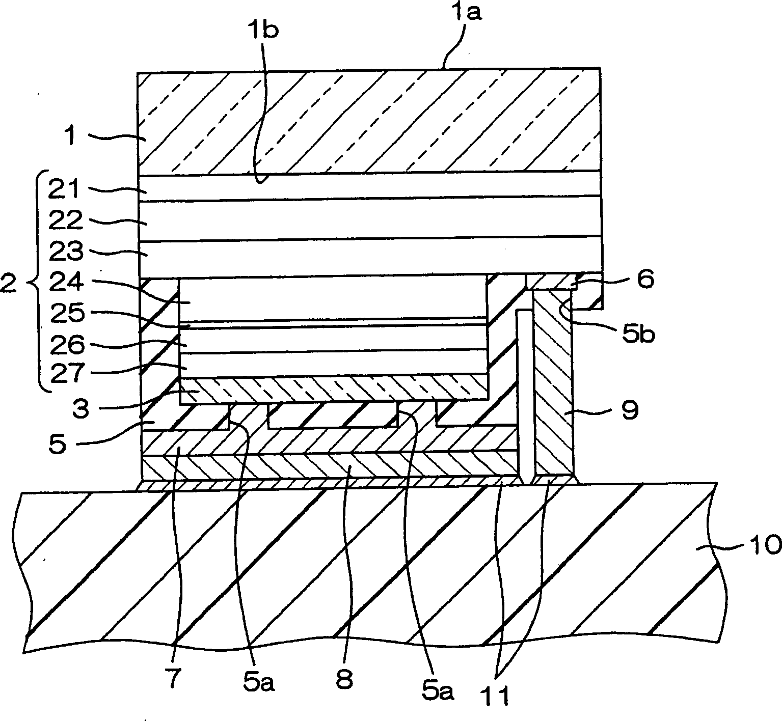
[0032] figure 1 It is a cross-sectional view diagrammatically showing the structure of a light emitting diode element according to an embodiment of the present invention. This light emitting diode element is a flip-chip type element, and includes: a sapphire substrate 1 as a transparent substrate, an InGaN semiconductor light emitting portion 2 formed on the sapphire substrate 1 , and a side of the InGaN semiconductor light emitting portion 2 opposite to the sapphire substrate 1. The P-side transparent electrode 3 formed by covering the surface. In the sapphire substrate 1, one of the surfaces is used as the light extraction surface 1a, and the other surface thereof is used as the element formation surface 1b. An InGaN semiconductor light emitting portion 2 is formed on the element forming surface 1b.

[0033] The sapphire substrate 1 is an insulating substrate transparent to the emission wavelength (for example, 460 nm) of the InGaN semiconductor light emitting portion 2 . ...


PUM


Abstract

A semiconductor light-emitting device comprising a first contact layer of a first conductivity type, a second contact layer of a second conductivity type, and a semiconductor light-emitting unit sandwiched between the contact layers and having an active layer. The semiconductor light-emitting device further comprises a transparent electrode in an ohmic contact with the surface of the second contact layer while covering the substantially entire surface of the second contact layer and being transparent to the emission wavelength of the semiconductor light-emitting unit, and a metal reflection film arranged opposite to the substantially entire region of the transparent electrode while being electrically connected with the transparent electrode, for reflecting light emitted from the semiconductor light-emitting unit and transmitted through the transparent electrode toward the semiconductor light-emitting unit.

Description

technical field [0001] The present invention relates to semiconductor light-emitting elements such as gallium nitride-based light-emitting diodes. Background technique [0002] A blue light emitting diode element is configured, for example, by forming an InGaN semiconductor light emitting portion on the surface of a sapphire substrate and forming electrodes on the P side and N side of the InGaN semiconductor light emitting portion (see Patent Document 1 below). However, since the sapphire substrate is insulating, it is necessary to form both P-side and N-side electrodes on the side of the InGaN semiconductor light emitting part, and wires must be drawn from them. As a result, the light from the InGaN semiconductor light emitting portion is blocked by the electrodes and the like, and the light extraction efficiency is poor. [0003] This problem can be improved by employing a configuration of a flip-chip type in which an InGaN semiconductor light-emitting portion is bonded t...

Claims


Application Information

Patent Timeline
Patent Type & Authority Applications(China)
IPC IPC(8): H01L33/00H01L33/22H01L33/40H01L33/42H01L33/44H01L33/62
CPCH01L33/22H01L33/42H01L2924/0002H01L33/405H01L33/62H01L33/44H01L2924/00
Inventor 浅原浩和酒井光彦园部雅之西田敏夫
Owner ROHM CO LTD
Why Eureka
Try Eureka