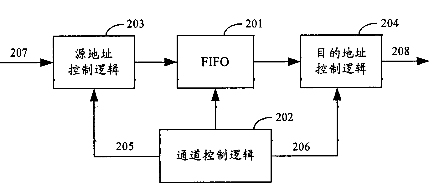
[0050] The core idea of this release is to improve the channel logic and the structure of each channel of the register group in the DMA, replace the FIFO control logic with the ping-pong operation structure, and realize the operation of different flow data through ping-pong switching, so that each channel of the DMA is independent It can simultaneously complete data reading and writing between peripherals and memory, forming a double DMA (DDMA, Duplicated DMA) structure.
[0051] In order to support the realization of the DDMA function, the DMA of the present invention has made two improvements to the existing DMA: first, a set of control registers is added corresponding to each channel; second, the implementation structure of the control logic of each DMA channel is changed and modified accordingly The structure of the channel control logic. Specifically: First, add four control registers for each channel to store the source address, destination address, control parameters and configuration parameters of the other transmission direction, including: DMAxSrcAddrl, used to indicate the source of the other transmission direction of channel x Address; DMAxDstAddr1, used to indicate the destination address of the other transmission direction of channel x; DMAxControl1, used to indicate the control parameters of the other transmission direction of channel x; DMAxConfig1, used to indicate the configuration parameters of the other transmission direction of channel x. Among them, x represents the channel number corresponding to the control register.
[0052] Second, design the control logic of each DMA channel as Figure 5 The implementation structure shown, such as Figure 5 As shown, the control logic of each channel in the present invention includes: channel control logic 501, state selection units 502 and 503, data buffers 504 and 505, source address control logic 203 and destination address control logic 204. Among them, the composition structure and function of the source address control logic 203 and the destination address control logic 204 are completely consistent with those in the existing DMA. Therefore, the channel control logic still uses the control signals 205 and 206 to control the source address control logic 203 and the destination address control logic respectively. 204 performs control, reads data from the source address to the DMA channel, and sends the data of the DMA channel to the destination address; and, the signals 207 and 208 indicate the data read from the source address and the data sent to the destination address, respectively. figure 1 The bus Master interface 105 is connected. The difference is that the source address in the present invention includes the sending address of the peripheral and the sending address of the memory. That is to say, the sending address from which the input signal 506 comes is actually the sending address of the peripheral or the sending address of the memory. , The receiving address to which the output signal 507 is sent is actually the receiving address of the memory or the receiving address of the peripheral. Figure 5 In, the channel control logic 501 controls the state switching of the state selection units 502 and 503 through the control signals 512 and 513, respectively, the state selection units 502 and 503 both include two state selections, and the states selected by the state selection units 502 and 503 are different; The state selection unit 502 stores the data in the data buffer 504 through the signal 508 in the first state, and stores the data in the data buffer 505 through the signal 510 in the second state; the state selection unit 503 passes the signal 511 in the first state Data is read from the data buffer 505, and in the second state, data is read from the data buffer 504 through a signal 509; the state selection units 502 and 503 can be implemented by a two-to-one selection circuit. The data buffers 504 and 505 are used to sequentially store the data to be transmitted. The data buffers into which the data is to be stored and the data buffers to be read are selected through signals 508 and 510, 509 and 511, respectively; data buffers 504 and 505 It can be realized by using a piece of RAM respectively.
[0053] based on Figure 5 In the structure shown, the process of data transmission between the peripheral and the memory is as follows: assuming that the data transmission from the peripheral to the memory is initiated first, the channel control logic 501 sets the state of the control selection unit 502 to the first state through the control signal 512 , Indicates that the data buffer 504 is selected to store data, and the state of the control selection unit 503 is set to the second state, indicating that the data in the data buffer 505 is selected to be read. At this time, the source address is the peripheral address, and the entry through 506 is Data sent by the peripheral. Then, after the address translation of the source address control logic, the data entering the DMA channel from the peripheral is stored in the data buffer 504, and at the same time, the data is read from the data buffer 505 and sent to the designated destination address. When the stored data reaches the set data volume, for example, the burst size of the burst transmission data volume is preset, the channel control logic 501 controls the state selection units 502 and 503 through the control signals 512 and 513 to perform state switching, and The state of the state selection unit 502 is switched to the second state, and the state of the state selection unit 503 is switched to the first state. At this time, the source address is the memory address, and the data sent through the memory is entered through 506. Then, the source address control logic Address translation, the data entering the DMA channel from the memory is stored in the data buffer 505, and at the same time, the data sent by the peripheral is read from the data buffer 504 and sent to the designated destination address of the memory. When the incoming data reaches the set amount of data again, the channel control logic 501 again controls the state selection units 502 and 503 through the control signals 512 and 513 to switch the state, and at the same time the source address changes, and so on, until all the data to be transmitted are processed. The data.
[0054] It should be noted that during the cycle operation, the data buffer 504 is actually used to store the data from the peripheral to the memory, and the data buffer 505 stores the data from the memory to the peripheral. In each operation cycle, one direction is completed at the same time. For the storage of data and the reading of data in the other direction, the size of the data buffer 504 and the data buffer 505 can be the same or different, so that a single-channel two-way data transmission is realized. Of course, in the first operating cycle, since data has not been officially stored in the data buffer 505, the data in the data buffer 505 is invalid and needs to be discarded. In addition, it is not limited to initiate the data transfer from the peripheral to the memory first, or to initiate the data transfer from the memory to the peripheral first; nor to limit the direction corresponding to each data buffer, as long as one data buffer serves data in one direction That's it.
[0055] It can be seen that the function and structure of the channel control logic 501 in the present invention and the channel control logic 202 in the prior art are different, mainly that the control of the state selection units 502 and 503 is added, and other functions are basically unchanged. The specific implementation of the channel control logic 501 to the state selection unit 502 and 503 is as follows: Figure 6 As shown, the channel control logic 501 adds a counter 601, a comparator 602, a switching control unit 603, and an inverter 604 on the basis of the existing channel control logic 202. Figure 6 Where 605 is the transmission count pulse from the bus Master interface 105. Here, the sending count is used. Every time the bus Master interface 105 sends a number, a count pulse 605 is generated to the counter; then, the counter 601 sends the count result 606 to the comparator 602 ; 607 is the data size Burst Size of a burst transmission set by the system. If the count value of the counting result 606 reaches the Burst Size, the comparator 602 generates a pulse signal 608, which is sent to the counter 601 on the one hand, Clear 601, and send it to the switching control unit 603 on the other hand to implement switching control; each time the switching control unit 603 receives a pulse signal 608, it inverts the control signal 512 output by itself to achieve the first state Switching between the second state and the second state; the control signal 512 output by the switching control unit 603 is directly used to control the state selection unit 502, and at the same time, the control signal 512 is sent to the inverter 604, and the control signal 513 is generated after inversion , Used to control the state selection unit 503.
[0056] based on Figure 5 with Figure 6 The working principle of the DMA channel control logic is shown, such as Figure 7 As shown, it is assumed that each DMA channel includes two data paths: path A and path B. Path A represents the DMA transfer from peripheral to memory, and path B represents the DMA transfer from memory to peripheral; the source address of path A is 304, the destination address is storage space 701, the source address of path B is storage space 702, and the destination address is 304; and set the burst size of path A to Burst_A, and the burst size of path B to Burst_B. Generally, the sizes of Burst_A and Burst_B are close . Figure 7 , The peripheral 304 and CPU305 are the same as the prior art, and DMA703 includes Figure 5 with Figure 6 The shown channel control logic structure of the DMA, except that the structure of each DMA channel is changed, other components are exactly the same as the prior art, the dotted line is the control signal, the solid line is the data signal from the peripheral to the memory, and the dashed line is Data signal from memory to peripheral. In addition, two storage spaces must be set up, which are used as the first data buffer when transferring data from the peripheral to the memory and the second data buffer when transferring data from the memory to the peripheral. Before DMA transfer, the CPU configures all the configuration parameters and control parameters of the peripherals and DMA. The process of implementing DMA transfer between peripherals and memory by using the DMA of the present invention is as follows:
[0057] a3) First initiate the DMA transfer of channel A, read the data to be transferred from the peripheral 304 into the first data buffer of the current DMA channel, and determine whether the amount of data currently read is equal to Burst_A, when the amount of data read When the size of a Burst_A is reached, the transmission is switched;
[0058] b3) Initiate the DMA move of channel B, read the data to be transferred from the storage space 702 to the second data buffer of the current DMA channel, and at the same time, read the data from the first data buffer of the current DMA channel to the storage Space 701, and judge whether the currently read data volume is equal to Burst_B, when the read data volume reaches a Burst_B size, the transmission switch is performed again;
[0059] c3) Read the data to be transferred from the peripheral 304 to the first data buffer of the current DMA channel. At the same time, read the data from the second data buffer of the current DMA channel to the peripheral 304, and judge the current read Whether the amount of data is equal to Burst_A, when the amount of read data reaches the size of a Burst_A, the transmission is switched;
[0060] d3) Read the data to be transferred from the storage space 702 to the second data buffer of the current DMA channel. At the same time, read the data from the first data buffer of the current DMA channel to the storage space 701, and judge the current read Is the amount of data equal to Burst_B? When the amount of read data reaches the size of a Burst_B, the transmission is switched again;
[0061] e3) Repeat the data transmission of steps c3 and d3 until the data transmission of channel A and channel B is completed.
[0062] Of course, in actual applications, it is not limited to initiate the DMA transfer of channel A first, or initiate the DMA transfer of channel B first.
[0063] The above are only preferred embodiments of the present invention, and are not used to limit the protection scope of the present invention.