Semiconductor device and method for making the same

A manufacturing method and semiconductor technology, applied in the fields of semiconductor/solid-state device manufacturing, semiconductor devices, semiconductor/solid-state device components, etc., can solve the problems of MCM reliability or yield deterioration, and prevent reliability or yield reduction. Effect

Inactive Publication Date: 2006-09-20
SONY CORP
View PDF3 Cites 3 Cited by
  • Summary
  • Abstract
  • Description
  • Claims
  • Application Information

AI Technical Summary

Problems solved by technology

[0010] These problems of electrostatic damage or plasma damage cause the reliability and yield of MCM to deteriorate, so it is a problem

Method used


Image

  • Semiconductor device and method for making the same
  • Semiconductor device and method for making the same
  • Semiconductor device and method for making the same

Examples


no. 1 Embodiment approach

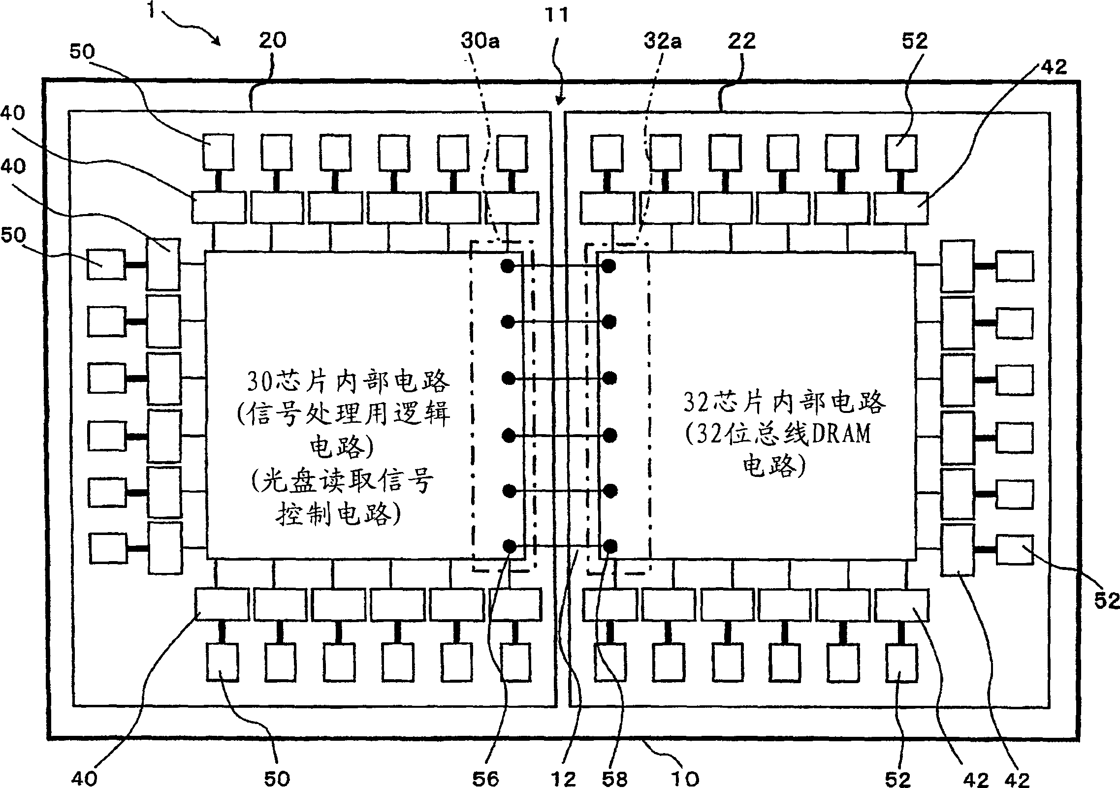
[0037] figure 1 It is a plan view showing the first embodiment of the semiconductor device to which the present invention is applied. The semiconductor device 1 shown in this figure mounts a plurality of substantially square ( figure 1 A so-called MCM type semiconductor device constituted by two) semiconductor chips 20 and 22 is shown in FIG.

[0038] Here, the first semiconductor chip 20 is, for example, a semiconductor chip for logic in which a logic circuit for signal processing is formed as the chip internal circuit 30 . On the other hand, the second semiconductor chip 22 is, for example, a semiconductor chip for a memory in which a DRAM (Dynamic RAM: Dynamic Random Access Memory) circuit forming a 32-bit bus is formed as the chip internal circuit 32 . Furthermore, the structure of the internal circuits 30 and 32 of the semiconductor chips 20 and 22 is not limited thereto.

[0039] For example, the semiconductor chips 20 and 22 are die-bonded on the support substrate 10...

no. 2 Embodiment approach

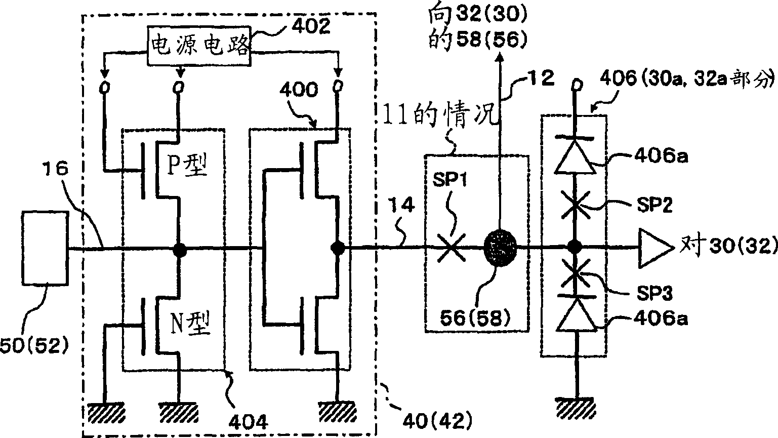
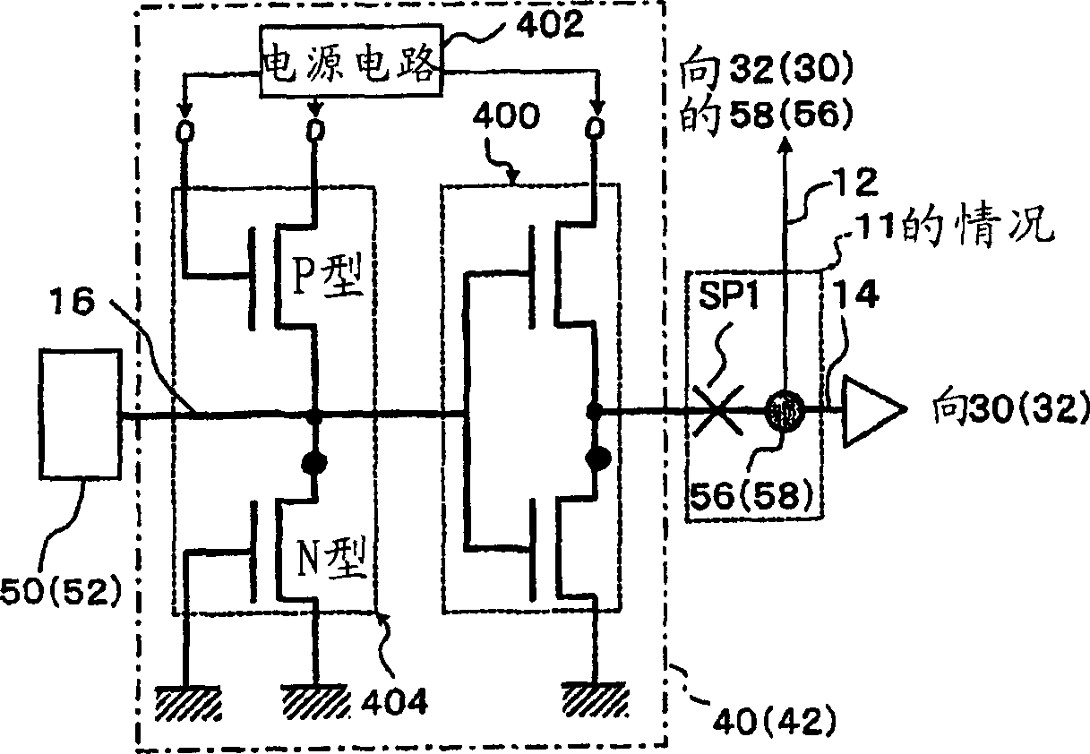
[0095] Figure 5A to Figure 5B It is a figure explaining the 2nd Embodiment of the semiconductor device to which this invention was applied. This figure is for the second embodiment Figure 3A to Figure 3C corresponding figure. The semiconductor device 1 of the second embodiment is characterized in that the protection circuit 406 can be disconnected from the signal line directly connected between the internal circuits 30 and 32 of the chip by using a switching circuit capable of turning on and off the input and output. to form. The semiconductor chips 20 and 22 differ only in that they have switching circuits, and the plan view of the semiconductor device 1 is basically the same as that of figure 1 Same as shown.

[0096] On the other hand, as the circuit structure of the inter-chip connection portion 11, for example, as shown in FIG. There is a switch circuit 408 between the circuits 406 that can switch between input and output. The switching circuit 408 is provided as ...

no. 3 Embodiment approach

[0101] Figure 6A to Figure 6B and Figure 7A to Figure 7B It is a figure explaining the 3rd embodiment of the semiconductor device to which this invention was applied. here, Figure 6A It is a plan view showing the third embodiment, and FIG. 6B is a sectional view taken along line A-A of the plan view. Figure 7A to Figure 7B shown to represent Figure 6A Details of the A-A line section of the floor plan.

[0102] like Figure 6A to Figure 6B and Figure 7A As shown, the semiconductor device 1 of the third embodiment is characterized in that the semiconductor chips 20 and 22 are face-down mounted using bumps. The rest of the configuration is substantially the same as that of the first or second embodiment, and a protection circuit 406 is provided on the signal line directly connected to the chip internal circuits 30 and 32 of the inter-chip connection portion 11 . The protection circuit 406 is the same as the first or second embodiment, and its purpose is to protect th...


PUM


Abstract

An MCM-type semiconductor device allowing high-speed operation and reduction in power consumption, and is also capable of preventing reliability and yield rate of MCM from degrading. The reduction in power consumption and increase in operation speed are attained by connecting signal lines between in-chip circuits (30), (32) in an electrically direct manner. On the signal line, a protection circuit (406) for electrostatic damage protection is provided. In device fabrication, connection using interconnections (12) between the in-chip circuits (30), (32) is carried out while keeping a protection circuit (406) connected to the signal lines (internal draw-out lines (12a), internal interconnections (14)), by which circuit components can be protected from static electricity even if electric charge accumulated on the semiconductor chips (20), (22) should flow into the signal lines, because the protection circuit (406) can absorb the charge. After the connection is completed, the protection circuit (406) can be disconnected from the signal lines, so as to avoid the protection circuit (406) to function as a load on the in-chip circuits (30), (32) during normal operation, and to thereby prevent the operation speed from decreasing.

Description

technical field [0001] The present invention relates to a semiconductor device and its manufacturing method. More specifically, it relates to a semiconductor device to which a so-called multi-chip module (MCM: Multi-Chip Module) technique is applied, in which a plurality of semiconductor chips are assembled as one electronic component, and a method for manufacturing the same. Background technique [0002] In response to demands for miniaturization, light weight, and low power consumption of electrical products, mounting technologies for mounting these semiconductor elements at a high density are being developed together with high integration technologies for semiconductor elements. In such a mounting technology, in order to achieve further high-density mounting, in addition to multilayer wiring support substrate or carrier chip mounting, it is being developed to mount multiple semiconductor elements (semiconductor chips) in advance as one electronic component on the same sup...

Claims


Application Information

Patent Timeline
Patent Type & Authority Applications(China)
IPC IPC(8): H01L23/12H01L25/04H01L23/52H01L27/04H01L21/822H01L23/62H01L25/065
CPCH01L2224/04042H01L25/0655H01L2924/15311H01L23/62H01L2224/0401H01L2224/16225H01L2224/16145H01L2224/73207H01L2924/157H01L2924/19107H01L2924/15192H01L23/12H01L25/04
Inventor 岩渊信
Owner SONY CORP
Why Eureka
Try Eureka