SOI structure with low k dielectric buried layer and its power device

A dielectric buried layer and power device technology, applied in the direction of electric solid state devices, semiconductor devices, electrical components, etc., can solve the problems of not being able to improve the vertical withstand voltage

Inactive Publication Date: 2006-10-11
UNIV OF ELECTRONIC SCI & TECH OF CHINA
View PDF0 Cites 16 Cited by
  • Summary
  • Abstract
  • Description
  • Claims
  • Application Information

AI Technical Summary

Problems solved by technology

Although the literature "Jeon B C., Kin D.Y., Lee Y S, et al.Buried air gap Structure for improving the breakdown voltage of SOI power MOSFET's.PowerElectronics and Motion Control Conference, 2000.Proceedings.PIEMC 2000.15-18 Aug.2000, Vol .3: 1061-106

Method used


Image

  • SOI structure with low k dielectric buried layer and its power device
  • SOI structure with low k dielectric buried layer and its power device
  • SOI structure with low k dielectric buried layer and its power device

Examples


Embodiment Construction

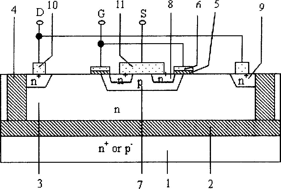
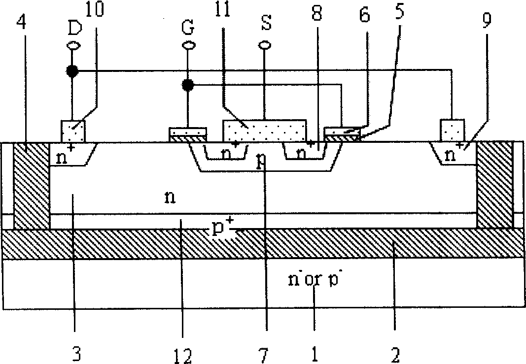
[0062] The low-k dielectric buried layer SOI structure provided according to the present invention includes VLk SOI structure, Lk SOI structure, VLk PSOI structure, and Lk PSOI structure, which can be used to produce various new structure power devices with excellent performance, including lateral double diffusion field Common power devices such as effect transistors, lateral insulated gate bipolar power transistors (LIGBT), PN diodes, and lateral thyristors. form VLk SOI LDMOS devices (such as Figure 7 shown), Lk SOI LDMOS devices (such as Figure 8 shown), VLk PSOUILDMOS devices (such as Figure 9 shown), LkPSOI LDMOS devices (such as Figure 10 shown), VLk SOI IGBT, Lk SOIIGBT, VLk PSOI IGBT, Lk PSOI IGBT, VLk SOI PN junction diode, Lk SOI PN junction diode, VLkPSOI PN junction diode, Lk PSOI PN junction diode, VLk SOI lateral thyristor, Lk SOI lateral thyristor Thyristor, VLkPSOI Lateral Thyristor, Lk PSOI Lateral Thyristor. With the development of semiconductor devic...


PUM


Abstract

The disclosed SOI power device with VLk SOI, Lk SOI, VLk PSOI and Lk PSOI four structures apples the low-k (dielectric coefficient) material to increase longitudinal electric field strength of the buried layer and modulate Si active electric field by the additional field on variable-k layer interface, while decrease the capacitor between drift region and substrate to improve on-off speed. This invention can be used to lots of new high pressure-resistant devices, such as lateral dual-diffusion FET, PN diode, etc.

Description

technical field [0001] The SOI power device structure and power device with a low dielectric coefficient dielectric buried layer belong to the technical field of semiconductor power devices, and in particular relate to the technical field of SOI (Semiconductor On Insulator) power device withstand voltage. Background technique [0002] Power devices with SOI (Silicon on Insulator) structure (SOI power devices for short) have higher operating speed, better insulation performance, stronger radiation resistance and no thyristor self-locking effect, so SOI power devices are used in Applications in the VLSI field have received widespread attention. The breakdown voltage of an SOI power device depends on the lower of the lateral breakdown voltage and the vertical breakdown voltage. The lateral withstand voltage design of SOI power devices follows the mature principle and technology of Si-based device lateral withstand voltage design, but due to the limitations of structure and pro...

Claims


Application Information

Patent Timeline
IPC IPC(8): H01L27/12H01L29/06H01L29/78H01L29/786H01L29/739H01L29/74H01L29/861
Inventor 罗小蓉李肇基张波
Owner UNIV OF ELECTRONIC SCI & TECH OF CHINA
Why Eureka
Try Eureka