Constant current circuit and flat display device
A constant current circuit and circuit technology, applied in the direction of circuits, electric light sources, electrical components, etc., can solve problems such as increased power consumption, and achieve the effect of reducing changes
- Summary
- Abstract
- Description
- Claims
- Application Information
AI Technical Summary
Problems solved by technology
Method used
Image

Examples
Embodiment 1
[0036] (1-1) Structure of Embodiment 1
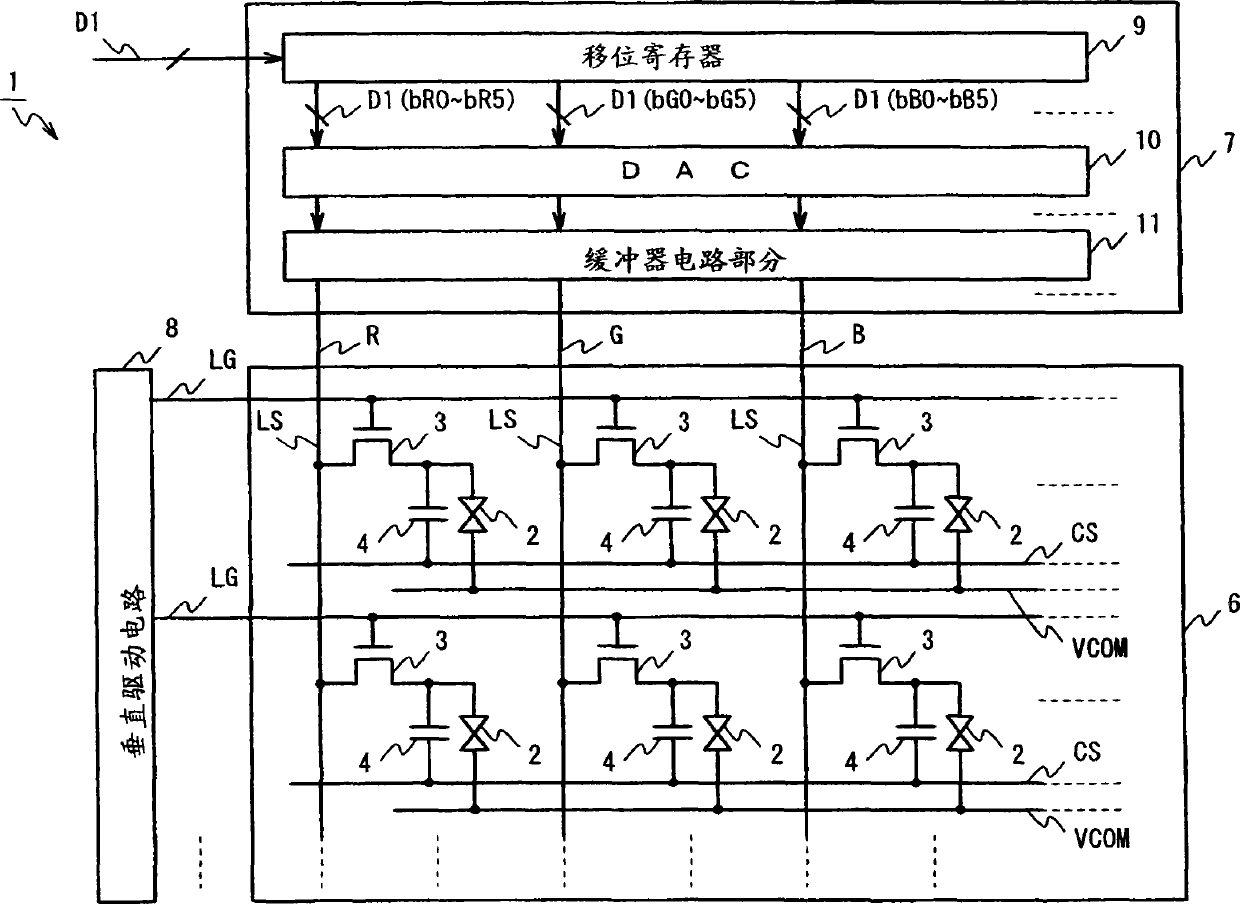
[0037] FIG. 3 shows a block diagram of a liquid crystal display device according to Embodiment 1 of the present invention. In this liquid crystal display device 1 , each pixel is formed of a liquid crystal cell 2 , a polysilicon TFT 3 which is a switching device of the liquid crystal cell 2 , and a storage capacitor 4 , and the pixels are arranged in a matrix to form a display section 6 . In this liquid crystal display device 1, each pixel which forms a display portion 6 is connected to a horizontal driving circuit 7 and a vertical driving circuit 8 through a signal line LS and a gate line LG, so that pixels are sequentially selected by means of the vertical driving circuit 8. And according to the driving signal from the horizontal driving circuit 7, the gray level of each pixel is set to display a desired image.
[0038] Accordingly, the vertical drive circuit 8 sequentially selects pixels in row units in conjunction with the processi...
Embodiment 2
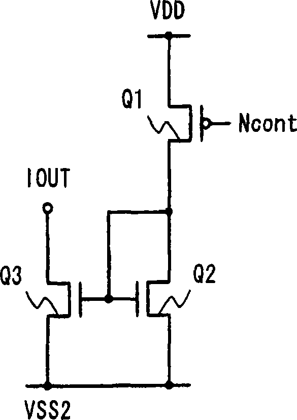
[0081] FIG. 14 shows a structural block diagram of an analog buffer circuit applied to a liquid crystal display according to Embodiment 2 of the present invention. The analog buffer circuit 40 is constructed of a PMOS source follower circuit instead of its analog buffer based on the NMOS source follower circuit according to Embodiment 1. Therefore, in the liquid crystal display according to Embodiment 2, precharge processing associated with switching between the ground potential and the negative predetermined potential is performed instead of the ground potential and the positive potential in the liquid crystal display device 1 according to Embodiment 1. Precharge processing associated with switching between predetermined potentials.
[0082]The analog buffer circuit 40 is constructed in the same manner as the analog buffer circuit 20 of Embodiment 1, except that its structure uses a PMOS transistor instead of an NMOS transistor, and except for the respective parts associated ...
Embodiment 3
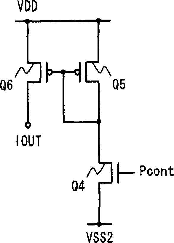
[0086] FIG. 17 shows a structural block diagram of an analog buffer circuit applied to a liquid crystal display according to Embodiment 3 of the present invention. The analog buffer circuit 50 is constructed by a combination of an NMOS source follower circuit and a PMOS source follower circuit instead of its analog buffer based on the NMOS source follower circuit according to Embodiment 1. Therefore, in the liquid crystal display according to Embodiment 3, its precharge processing associated with switching between the ground potential and a negative predetermined potential is performed instead of its connection to the ground potential in the liquid crystal display device 1 according to Embodiment 1. Precharge processing associated with switching between positive predetermined potentials.
[0087] As shown in FIG. 18 , the analog buffer circuit is constructed by a combination of its source follower circuit using NMOS transistors according to Embodiment 1 and its source follower...
PUM
 Abstract
Description
Claims
Application Information
 - R&D
- Intellectual Property
- Life Sciences
- Materials
- Tech Scout
- Unparalleled Data Quality
- Higher Quality Content
- 60% Fewer Hallucinations
Browse by: Latest US Patents, China's latest patents, Technical Efficacy Thesaurus, Application Domain, Technology Topic, Popular Technical Reports.
© 2025 PatSnap. All rights reserved.Legal|Privacy policy|Modern Slavery Act Transparency Statement|Sitemap|About US| Contact US: help@patsnap.com