Check patentability & draft patents in minutes with Patsnap Eureka AI!

Chip architecture with multiple functions

A multi-functional, chip technology, applied in the direction of electrical components, electrical solid devices, circuits, etc., can solve the problems of product elastic cost reduction, product inelasticity, unfavorable effective cost, etc., and achieve the goal of avoiding volume, reducing volume, and reducing cost Effect

Inactive Publication Date: 2006-11-15
HOLTEK SEMICON
View PDF0 Cites 3 Cited by
  • Summary
  • Abstract
  • Description
  • Claims
  • Application Information

AI Technical Summary

Problems solved by technology

Although this point can be simplified in the manufacturing process, it is not flexible in the production of products, and it is not conducive to effective cost reduction.
Moreover, when faced with different memory capacity or characteristic requirements, considering a single process, the chip itself must be additionally designed with non-volatile memory of different memory capacity or type, which is not conducive to the flexibility and flexibility of the product in production. cost reduction

Method used


Image

  • Chip architecture with multiple functions
  • Chip architecture with multiple functions
  • Chip architecture with multiple functions

Examples


Embodiment Construction

[0039] In order to have a further cognition and understanding of the features, purposes and functions of the present invention, the detailed description is as follows in conjunction with the accompanying drawings:

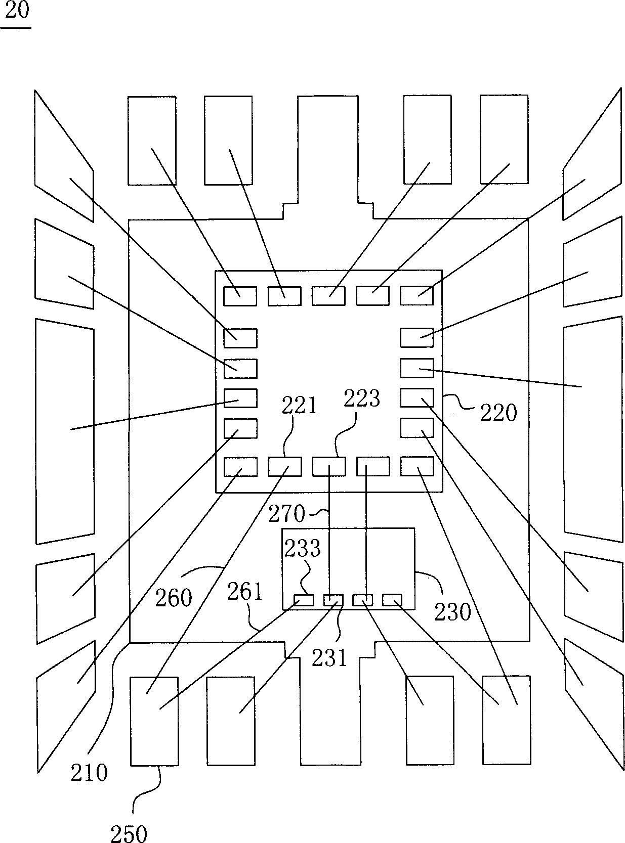
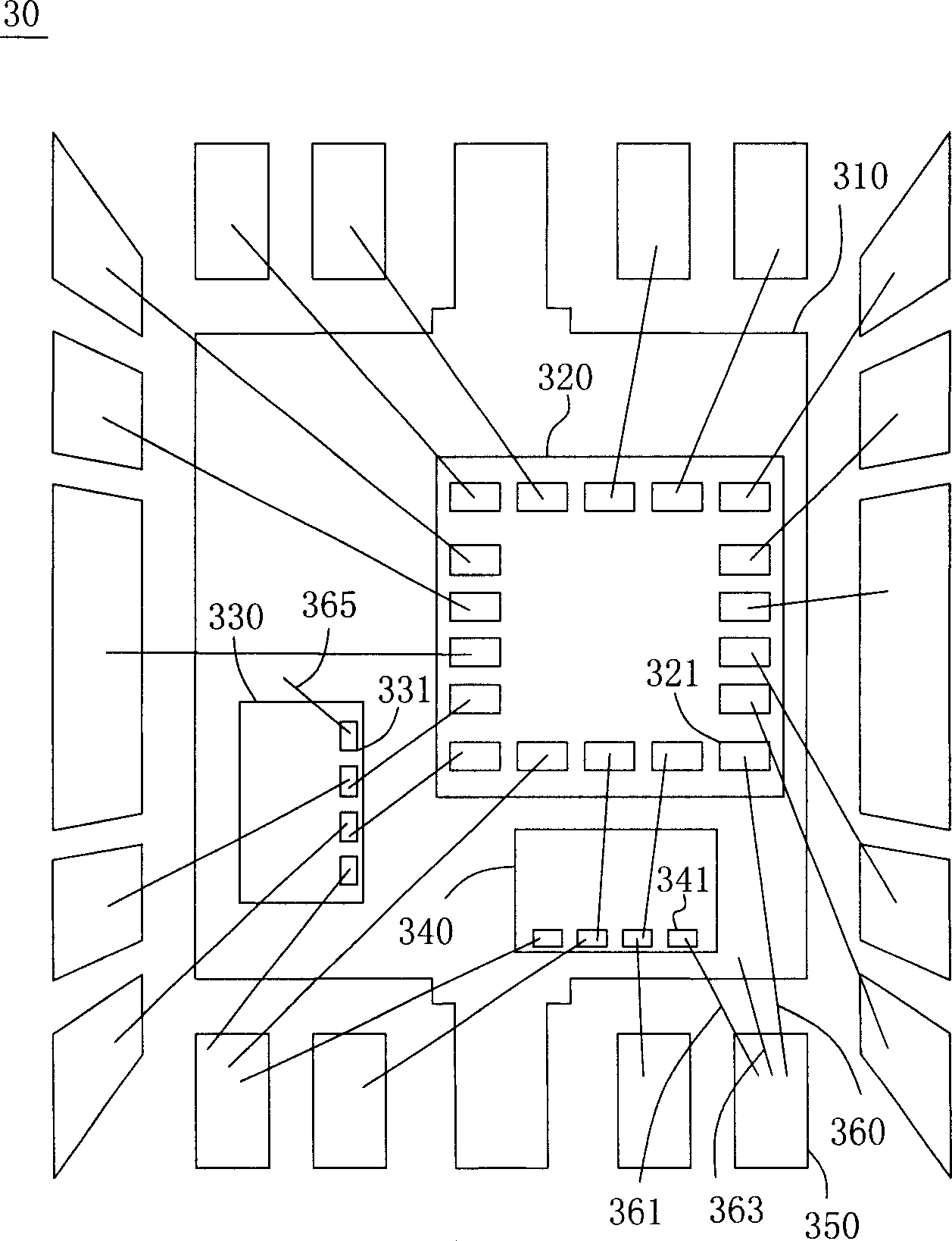
[0040] Please refer to figure 1 , figure 1 It is a schematic diagram of the multifunctional chip architecture of the present invention. The outside of the chip structure 10 is covered by a package (not shown), and the inside of the package mainly includes a chip holder 110 , a microcontroller 120 and a non-volatile memory 130 on the chip holder. In particular, the microcontroller 120 and the non-volatile memory 130 can choose to adopt different processes.

[0041] The advantage of using different processes for the microcontroller 120 and the non-volatile memory 130 is that when the chip architecture 10 is actually operating, the degree of current or voltage that the microcontroller 120 and the non-volatile memory 130 bear is not proportional to the scale. The sa...


PUM


Abstract

This invention relates to multifunctional chip structure that its outside is coated by a packaging body. It includes a chip seat, a first chip is set on the seat, and the first chip has control function. At least one second chip set on the seat and beside the first chip, it has preset function. Several pins set around the chip, so the signal output from the first and second chip can be extracted out the packaging body; the pin number is same to the situation of the first chip packaged. Several throwing mat are set on the two chips, and at least any two mats are common online of the two chips. Several throwing are welded to the mat, pins said above, and between the chip seat to make signal connecting between the first chip, second chip, pins and the chip seat.

Description

technical field [0001] The present invention relates to a multi-functional chip architecture, in particular to a chip architecture with multiple chips and different manufacturing processes among the chips. Background technique [0002] So far, most microcontroller chips or microprocessor chips have no built-in non-volatile memory in their packages, so after the products containing these chips are powered off, these chips cannot actively retain the stored data . Products containing these chips must store the data stored in the chip through non-volatile memory, such as electrically erasable read-only memory (EEPROM), flash memory (Flashmemory), magnetic memory (MRAM), etc. stored data. In other words, some current products containing microcontroller chips or microprocessor chips must additionally use non-volatile memory outside the package to store data after the product is powered off. Under the above circumstances, not only the cost of the chip and the external memory is ...

Claims


Application Information

Patent Timeline
IPC IPC(8): H01L25/00H01L23/50
CPCH01L2224/05553H01L2224/48137H01L2224/48247H01L2224/48257H01L2224/49171H01L2224/49175H01L2924/00
Inventor 叶秉霖
Owner HOLTEK SEMICON
Features
  • R&D
  • Intellectual Property
  • Life Sciences
  • Materials
  • Tech Scout
  • Unparalleled Data Quality
  • Higher Quality Content
  • 60% Fewer Hallucinations
Learn More