Semiconductor device and process for fabricating the same

A manufacturing method and semiconductor technology, applied in semiconductor/solid-state device manufacturing, semiconductor devices, semiconductor/solid-state device components, etc., can solve problems such as increased impedance, high cost, and thinning limitations

Active Publication Date: 2010-04-28
TAIWAN SEMICON MFG CO LTD
View PDF3 Cites 0 Cited by
  • Summary
  • Abstract
  • Description
  • Claims
  • Application Information

AI Technical Summary

Problems solved by technology

However, as the number of welding lines increases, the number of processes also becomes longer
In addition, the connection path becomes longer and the impedance increases due to the bonding wire, which may lead to deterioration of characteristics (high-speed operation)
Furthermore, there is a problem with the processing of the thinned bare chip (Bare Chip), and there are limitations in the overall thinning
[0013] (3) In order to improve the yield of finished products, the final test must be carried out with bare chips before installation (stacking); : known good chip) the cost of the final test is very high
[0014] (4) When stacking multiple positions on one chip, the maximum of 2 layers is already the limit, and even so, the connection path will become longer, which will easily affect the characteristics

Method used


Image

  • Semiconductor device and process for fabricating the same
  • Semiconductor device and process for fabricating the same
  • Semiconductor device and process for fabricating the same

Examples


Embodiment 1

[0157] Figure 1 to Figure 20 It is a diagram related to the stacked semiconductor device according to the first embodiment of the present invention. Figure 1 to Figure 3 is a diagram related to the structure of a stacked semiconductor device, Figure 4 to Figure 19 is a diagram related to the manufacture of a stacked semiconductor device, Figure 20 It is a diagram showing a mounted state of a stacked semiconductor device.

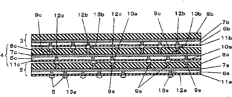
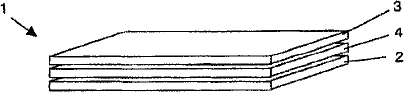
[0158] Such as figure 2 As shown, the stacked semiconductor device 1 manufactured by the manufacturing method of the present invention includes: a quadrangular first semiconductor device 2 located at the next level, a first semiconductor device 2 located at an intermediate level and fixedly stacked on the upper surface of the first semiconductor device 2 3 semiconductor device 4, the second semiconductor device 3 positioned on the upper stage and fixedly stacked on the upper surface of the third semiconductor device 4. In the stacked semiconductor d...

Embodiment 2

[0226] Figure 21 It is a cross-sectional view schematically showing a stacked semiconductor device according to Embodiment 2 of the present invention. In the second embodiment, in the gap between the first semiconductor device 2 and the third semiconductor device 4 and in the gap between the third semiconductor device 4 and the second semiconductor device 3 in the stacked semiconductor device 1 of the first embodiment An insulating resin is filled to form underfill layers 50 and 51 . The voids are buried by the underfill layers 50 , 51 , so that short-circuit failures due to foreign matter contamination or the like can be prevented. For example, polyimide resin is filled in the cavity as an insulating resin in a vacuum environment, and then baked to cure it.

Embodiment 3

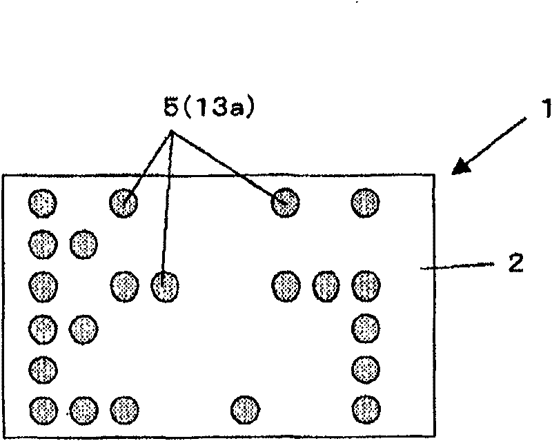
[0228] Figure 22 (a) and (b) are schematic cross-sectional views of a two-stage stacked fixed type stacked semiconductor device 1 according to Embodiment 3 of the present invention. Figure 22 In both (a) and (b), the semiconductor substrates 6a, 6b are placed on top, and the first insulating layers 8a, 8b are placed on the bottom to perform lamination and fixing. Both bump electrodes 10 a on the lower surface of the first semiconductor device 2 serve as external electrode terminals 5 . In addition, the bump electrodes 13a on the upper surface of the first semiconductor device 2 form a bonding body, and the second semiconductor device 3 is laminated and fixed. That is, the bump electrodes 13 a mounted on the penetration electrodes 12 a on the upper surface side of the first semiconductor device 2 are connected to the columnar electrodes 9 a on the lower surface of the second semiconductor device 3 .

[0229] In addition, in Figure 22 In (a), no electrodes are exposed on t...


PUM


Abstract

A thin stacked semiconductor device suitable for high speed operation. A plurality of specified circuits are formed on one surface of a semiconductor substrate while being arranged, and wiring and insulating layers being connected electrically with the circuits are laminated and formed sequentially in a specified pattern to form a multilayer wiring part. At the stage for forming the multilayer wiring part, a filling electrode is formed on the semiconductor substrate such that the surface is covered with an insulating film, a post electrode is formed on specified wiring at the multilayer wiringpart, a first insulating layer is formed on one surface of the semiconductor substrate, the surface of the first insulating layer is removed by a specified thickness to expose the post electrode, theother surface of the semiconductor substrate is ground to expose the filling electrode and to form a through-type electrode, forward end of the through-type electrode is projected by etching one surface of the semiconductor substrate, a second insulating layer is formed on one surface of the semiconductor substrate while exposing the forward end of the through-type electrode, bump electrodes areformed on both electrodes and then the semiconductor substrate is divided to form a semiconductor device. A plurality of semiconductor devices thus obtained are stacked and secured at the bump electrodesthus manufacturing a stacked semiconductor device.

Description

technical field [0001] The present invention relates to a thinner and faster-operating semiconductor device and its manufacturing method, and more particularly to an extremely efficient manufacturing technique for sequentially stacking a plurality of semiconductor devices to manufacture a stacked semiconductor device. Background technique [0002] Along with the development of various electronic devices in terms of multi-function and miniaturization, the semiconductor device embedded in the electronic device has gradually evolved into a structure in which many circuit elements are built in a small volume. As a method for increasing the integration density of semiconductor devices (integrated circuit devices), three-dimensional stacked semiconductor devices are known. [0003] For example, a structure for achieving high integration by stacking and fixing LSI chips having through-electrodes penetrating multiple stages on an interposer has been proposed (for example, Patent Doc...

Claims


Application Information

Patent Timeline
Patent Type & Authority Patents(China)
IPC IPC(8): H01L25/065H01L25/07H01L25/10H01L25/11H01L25/18H01L23/52H01L21/3205H01L23/538
CPCH01L2225/06513H01L2924/01327H01L2924/15311H01L2225/06541H01L25/0657H01L2224/16145H01L2924/10253H01L2924/3011H01L23/481H01L2224/16225H01L25/0652H01L2924/12044H01L2924/1461H01L2924/14H01L2224/13025H01L2224/1403H01L2224/16146H01L2224/16148H01L2224/17181H01L2224/81191H01L2224/81193H01L2224/05573H01L2224/05624H01L2224/05647H01L2224/05655H01L2224/05666H01L2224/05684H01L2924/00014H01L2224/0554H01L24/13H01L24/03H01L2224/0616H01L24/05H01L2924/00H01L2924/013H01L2224/05599H01L2224/0555H01L2224/0556H01L23/12H01L25/11H01L25/065H01L23/488H01L23/48H01L25/04H01L23/3157H01L23/49838H01L29/78
Inventor 石原政道
Owner TAIWAN SEMICON MFG CO LTD
Why Eureka
Try Eureka