

Method for extracting interconnection parasitic capacitance capable of automatically adapting process characteristic size
A technology of parasitic capacitance and extraction method, which is applied in the direction of circuits, electrical components, electrical digital data processing, etc., can solve problems such as poor self-adaptive ability, and achieve the effect of increasing speed
- Summary
- Abstract
- Description
- Claims
- Application Information
AI Technical Summary
Problems solved by technology
Method used
Image


Examples
Embodiment Construction
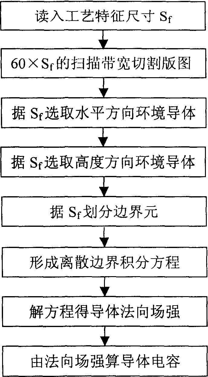
[0086] exist figure 1 In the shown embodiment, the utility model is carried out by the following steps of computer successively:
[0087] 1) Read the process feature size S of the input layout from the process file f . figure 2 A schematic diagram of the input layout.
[0088] 2) Scan the entire layout from left to right with a vertical scanning band.
[0089] The width W of the scanning band in this method sb Set to be proportional to the feature process size of the layout.
[0090] In this method, the scanning width W sb The recommended value is 60×S f .
[0091] The scanning tape stops at each station. Scan strip sites are the left and right endpoints of conductor edges and the intersections between conductor edges on the layout. When the scanning belt stops at each station, the following actions are performed:
[0092] a) Reads all conductors starting at the right end of the current swath into the memory worksheet.
[0093] b) All conductors ending at the left ...
PUM
 Abstract
Description
Claims
Application Information