Image
Click on the blue label to locate the original text in one second.
Reading with bidirectional positioning of images and text.
Examples
no. 1 example
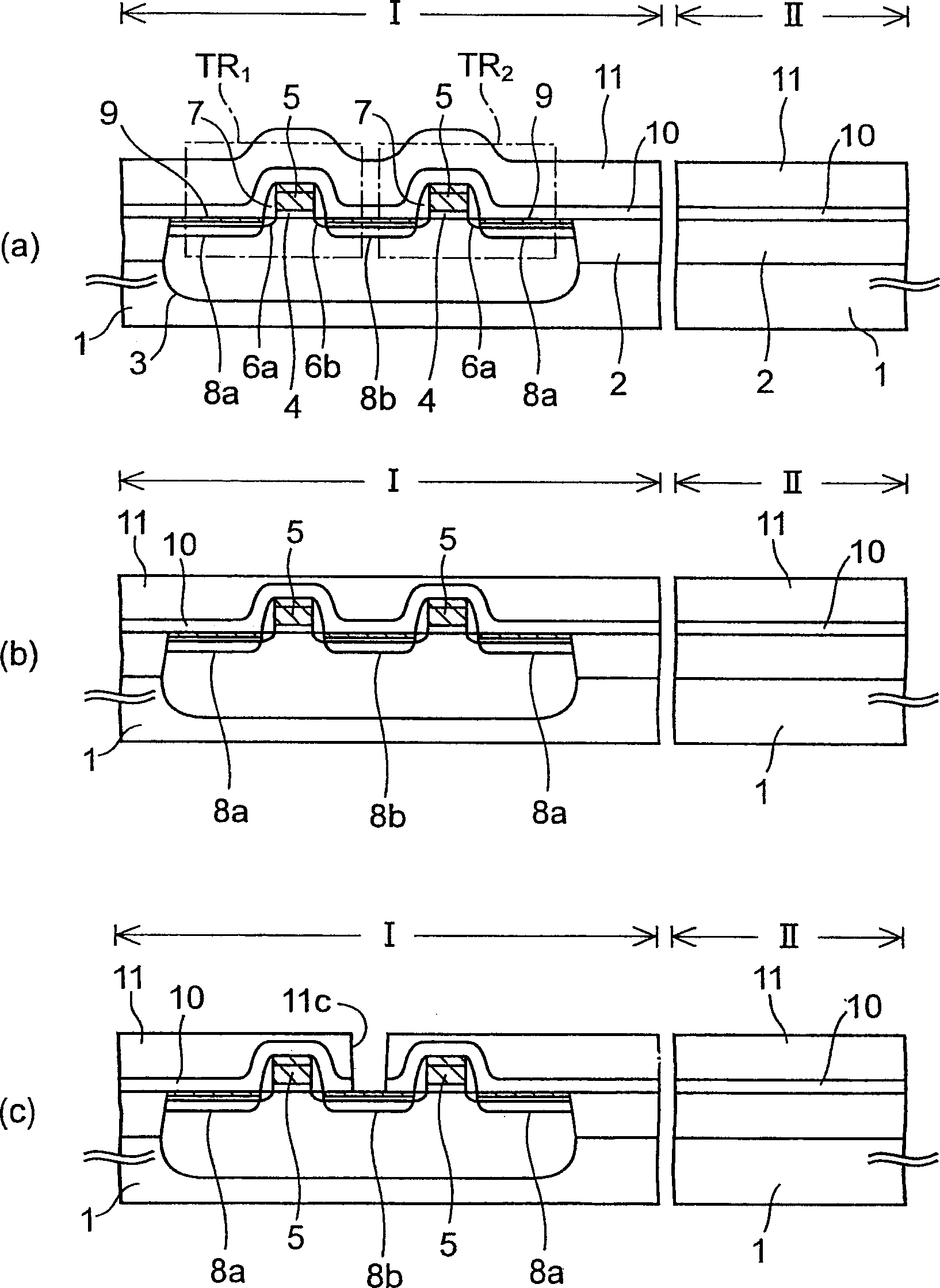
[0097] Figure 9-Figure 18 is a cross-sectional view of the semiconductor device in production according to the first embodiment of the present invention. Note that in these figures, the same reference numerals Figure 1-Figure 8 The components are the same as those in , and a detailed description thereof is subsequently omitted.
[0098] This semiconductor device is a stacked FeRAM, and is manufactured as follows.
[0099] First, execute in the manner described in "Preliminary Instructions" figure 1 Steps of (a) and (b). Next, if Figure 9 As shown in (a), the photoresist coated on the first insulating film 11 is exposed and developed to form a second resist pattern 30 .
[0100] As shown in the figure, hole-shaped first and second windows 30a, 30b are respectively formed in the second resist pattern 30 directly above the first and second source / drain regions 8a, 8b.
[0101] Subsequently, if Figure 9 As shown in (b), for example, a high-frequency current with a frequ...
no. 2 example
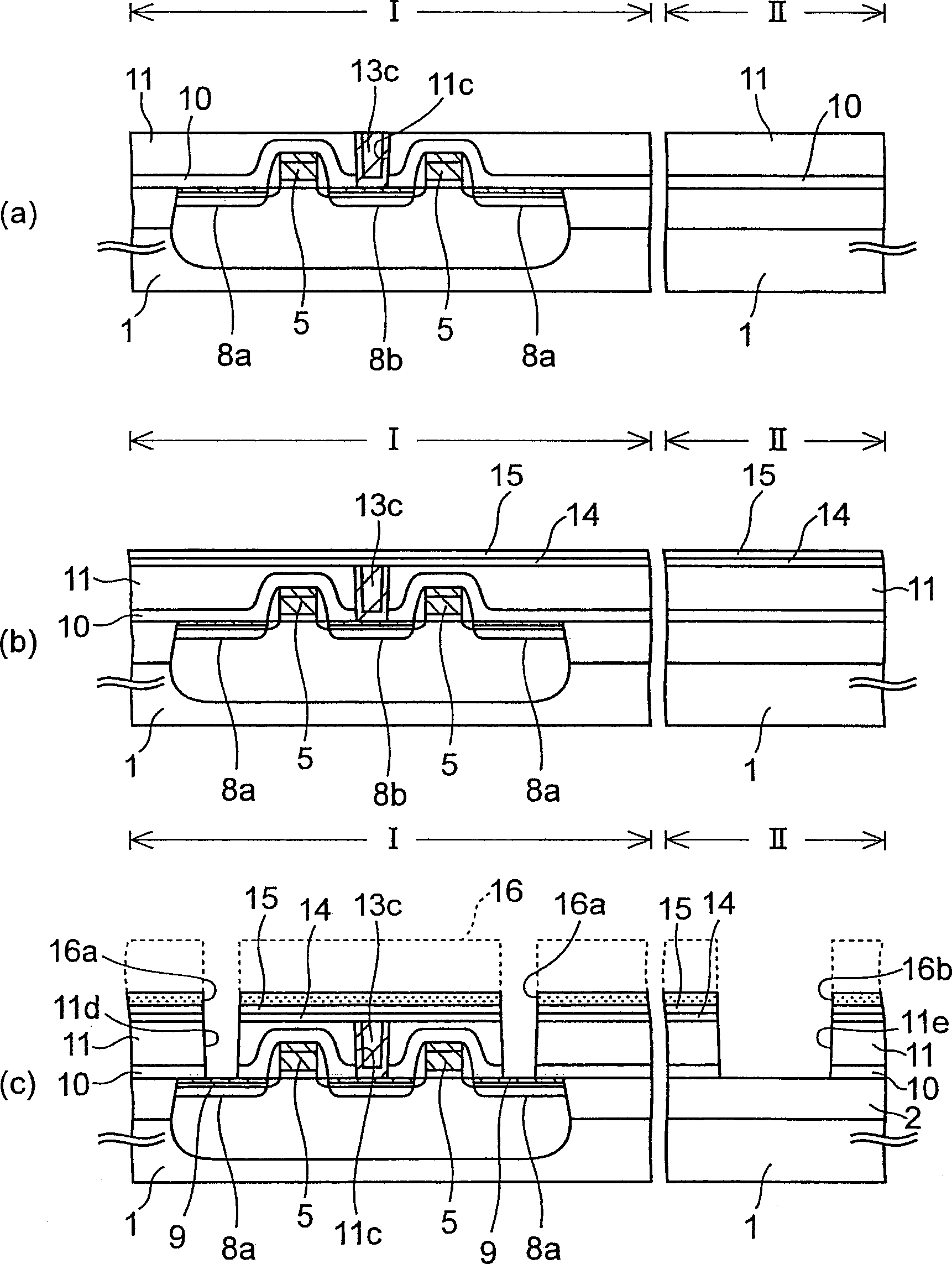
[0174] In the above first embodiment, if Figure 11 As shown in (b) and (c), the auxiliary conductive plug 36 a is composed of a laminated film of the second barrier metal film 35 and the conductive film 36 . In contrast, in the present embodiment, the auxiliary conductive plug 36 a is composed of the conductive film 36 only.
[0175] Figure 19 (a)- Figure 19 (c) is a cross-sectional view of a semiconductor device in production according to a second embodiment of the present invention. Note that in these figures, the same components as those described in the first embodiment are denoted by the same reference numerals, and a detailed description thereof is subsequently omitted.
[0176] In order to manufacture the semiconductor device according to the present embodiment, the method described in the first embodiment is carried out Figure 9 (a)- Figure 11 Steps shown in (a).
[0177] Subsequently, if Figure 19 As shown in (a), a single-layer conductive film 36 is form...
PUM
Abstract
To provide a semiconductor device capable of improving accuracy in finishing a hole in which a conductive plug right under a capacitor, and a manufacturing method of such a semiconductor device comprising the following steps: a step of forming first and second conductive plugs 32 a , 32 b in first and second holes 11 a , 11 b in a first insulating film 11; a step of forming a first opening 14 a in an oxidation preventing insulating film 14 ; a step of forming an auxiliary conductive plug 36 a in the first opening 14 a; a step of forming a capacitor Q on the auxiliary conductive plug 36 a; a step of forming third and fourth holes 41 a , 41 b in a second insulating film 41 covering the capacitor Q; a step of forming the second opening 14 b in the oxidation preventing insulating film 14 under the fourth hole 41 b; a step of forming a third conductive plug 47 a in the third hole 41 a; and a step of forming a fourth conductive plug 47 b in the third hole 41 a.
Description
[0001] References to related applications [0002] This application is based on and claims the benefit of priority from Japanese Priority Patent Application No. 2005-221010 filed on July 29, 2005, the entire contents of which are hereby incorporated by reference. technical field [0003] The invention relates to a semiconductor device and a manufacturing method thereof. Background technique [0004] Flash memory and ferroelectric memory are known non-volatile memories that retain information even when power is removed. [0005] Flash memory among these two types of memory has a floating gate embedded in the gate insulating film of an insulated gate field effecttransistor (IGFET), and this type of memory stores information by accumulating electric charge representing information and storing it in the floating gate . However, flash memory has a disadvantage in that a tunnel current needs to flow through a gate insulating film when writing or erasing information, which requi...
Claims
Application Information
Patent Timeline
Application Date:The date an application was filed.
Publication Date:The date a patent or application was officially published.
First Publication Date:The earliest publication date of a patent with the same application number.
Issue Date:Publication date of the patent grant document.
PCT Entry Date:The Entry date of PCT National Phase.
Estimated Expiry Date:The statutory expiry date of a patent right according to the Patent Law, and it is the longest term of protection that the patent right can achieve without the termination of the patent right due to other reasons(Term extension factor has been taken into account ).
Invalid Date:Actual expiry date is based on effective date or publication date of legal transaction data of invalid patent.
