Method for avoiding or reducing V-defect of blue-green light LED material

A light-emitting diode, blue-green light technology, applied in electrical components, circuits, semiconductor devices, etc., can solve problems such as large lattice mismatch and large difference in thermal expansion coefficient

Active Publication Date: 2007-01-31
HC SEMITEK SUZHOU
View PDF0 Cites 25 Cited by
  • Summary
  • Abstract
  • Description
  • Claims
  • Application Information

AI Technical Summary

Problems solved by technology

These materials have a large lattice mismatch with GaN and a large difference in thermal expansion coefficient, res

Method used


Image

  • Method for avoiding or reducing V-defect of blue-green light LED material
  • Method for avoiding or reducing V-defect of blue-green light LED material
  • Method for avoiding or reducing V-defect of blue-green light LED material

Examples


Embodiment 1

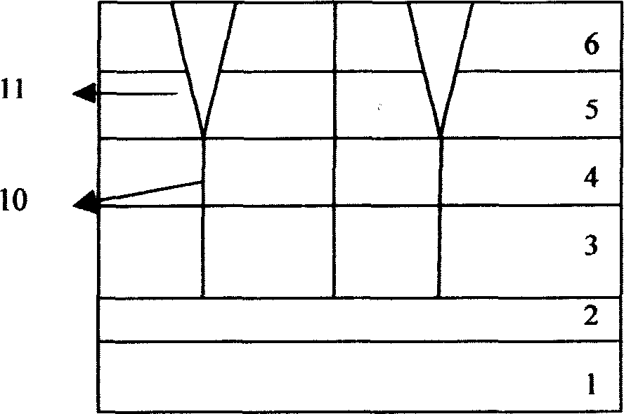
[0029] First, the substrate material sapphire Sapphire substrate layer 1 is desorbed and cleaned for 1 to 10 minutes at a temperature greater than 1100°C in a hydrogen atmosphere;

[0030] Lower the temperature to 500°C, and grow a 25nm-thick low-temperature GaN nucleation layer 2. During this growth process, the growth pressure is 200 Torr, and the V / III molar ratio is 5000;

[0031] Raise the substrate temperature to 1100°C, anneal the low-temperature GaN nucleation layer in situ, and the annealing time is 1 minute; after annealing, adjust the temperature to 1100°C, grow a 4 micron n-type doped GaN layer 3, The growth pressure is 200Torr, the V / III molar ratio is 3000, and the doping concentration is 1×10 19 cm -3 ;

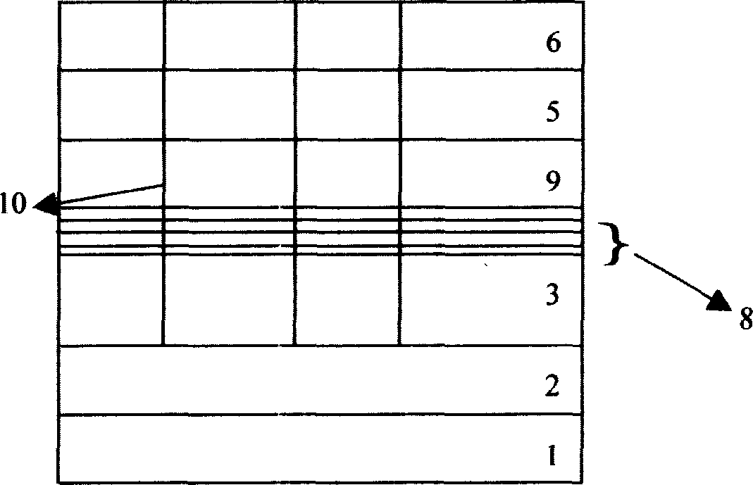
[0032] Adjust the temperature to a higher temperature region of 1120°C, and control the growth pressure at 75 Torr to grow n-type doped Al x Ga 1-x N / GaN (x=0.2) superlattice layer 8 structure, where Al 0.2 Ga 0.8 The thickness of the N layer is 2nm, the ...

Embodiment 2

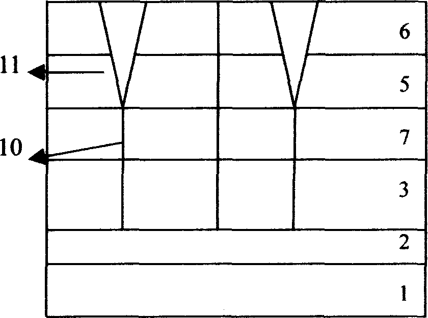
[0039] First, the substrate material sapphire Sapphire substrate layer 1 is desorbed and cleaned for 1 to 10 minutes at a temperature greater than 1100°C in a hydrogen atmosphere;

[0040] Lower the temperature to 500°C, and grow a 25nm-thick low-temperature GaN nucleation layer 2. During this growth process, the growth pressure is 200 Torr, and the V / III molar ratio is 5000;

[0041] Raise the substrate temperature to 1100°C, anneal the low-temperature GaN nucleation layer in situ, and the annealing time is 1 minute; after annealing, adjust the temperature to 1050°C, grow a 4 micron n-type doped GaN layer 3, The growth pressure is 200Torr, the V / III molar ratio is 3000, and the doping concentration is 1×10 19 cm -3 ;

[0042] Adjust the temperature to a higher temperature region of 1120°C, and control the growth pressure at 75 Torr to grow n-type doped Al x Ga 1-x N / GaN (x=0.1) superlattice layer 8 structure, where Al 0.2 Ga 0.8 The thickness of the N layer is 2nm, the ...

Embodiment 3

[0049] First, the substrate material sapphire Sapphire substrate layer 1 is desorbed and cleaned for 1 to 10 minutes at a temperature greater than 1100°C in a hydrogen atmosphere;

[0050] Lower the temperature to 500°C, and grow a 25nm-thick low-temperature GaN nucleation layer 2. During this growth process, the growth pressure is 200 Torr, and the V / III molar ratio is 5000;

[0051] Raise the substrate temperature to 1100°C, anneal the low-temperature GaN nucleation layer in situ, and the annealing time is 1 minute; after annealing, adjust the temperature to 1050°C, grow a 4 micron n-type doped GaN layer 3, The growth pressure is 200Torr, the V / III molar ratio is 3000, and the doping concentration is 1×10 19 cm -3 ;

[0052] Adjust the temperature to a higher temperature region of 1120°C, and control the growth pressure at 75 Torr to grow n-type doped Al x Ga 1-x N / GaN (x=0.1) superlattice layer 8 structure, where Al 0.2 Ga 0.8 The thickness of the N layer is 2nm, the ...


PUM

PropertyMeasurementUnit
Thicknessaaaaaaaaaa
Thicknessaaaaaaaaaa
Thicknessaaaaaaaaaa

Abstract

The invention is a method for avoiding or reducing V-type defect of blue-green light emitting diode material which has in turn sapphire substrate, low-temperature grown GaN buffer layer, high-temperature grown n-GaN layer, InGa1-Yn/GaN multi-quantum trap layer, and p-Alx Ga1-xN/ p-GaN layer, characterized in that: there is a grown n-AlxGa1-xN/GaN superlattice layer between the high-temperature grown n-GaN layer and InGa1-Yn/GaN multi-quantum trap layer, where 0<x<1, the growth temperature is between 1100deg.C and 1200deg.C, the pressure is 30Torr-100Torr, the AlxGa1-xN layer is 1nm-5nm thick, the GaN layer is 1nm-5nm thick, the periodicity is 5-10, the doping concentration is between 1*1016cm-3 and 1*1018cm-3; there is also a weak n-type doped GaN layer between the high-temperature grown n-GaN layer and InGa1-Yn/GaN multi-quantum trap layer, where the growth temperature is 1150 deg.C-1200 deg.C, the growth pressure is 30Torr-80Torr, and the thickness is 1m-50nm, the doping concentration is between 1*1016cm-3 and 5*1017cm-3. And it can avoid or reduce V-type defect and reverse leakage current generated by this.

Description

technical field [0001] The invention relates to a method for epitaxial growth of GaN-based blue-green light-emitting diodes by metal-organic source chemical vapor deposition on a sapphire heterogeneous substrate, in particular to a method for avoiding or reducing the generation of V-type defects and the resulting reverse method of leakage current. Background technique [0002] The third-generation semiconductor materials group III nitrides include InN, GaN, AlN and their alloys InGaN, AlGaN and AlInGaN materials have excellent and unique photoelectric properties, so they have received extensive attention. Group III nitride materials are semiconductor materials with direct bandgap and wide energy band. Their direct bandgap is continuously adjustable from 0.79eV to 6.2eV, corresponding to the infrared to deep ultraviolet band of electromagnetic waves, and the main applications are blue, green to deep ultraviolet. Light-emitting devices, detection devic...

Claims


Application Information

Patent Timeline
IPC IPC(8): H01L33/00
Inventor 刘伟
Owner HC SEMITEK SUZHOU
Why Eureka
Try Eureka