Method of manufacturing a semiconductor structure and a corresponding semiconductor structure

A semiconductor and body region technology, applied in the fields of semiconductor devices, semiconductor/solid-state device manufacturing, semiconductor/solid-state device components, etc., can solve problems such as functional damage and impact, and achieve the effect of minimizing the risk of damage

Inactive Publication Date: 2007-02-07
QIMONDA
View PDF0 Cites 8 Cited by
  • Summary
  • Abstract
  • Description
  • Claims
  • Application Information

AI Technical Summary

Problems solved by technology

Therefore, it may cause damage or affect the function of the chip (for example, memory chip)

Method used


Image

  • Method of manufacturing a semiconductor structure and a corresponding semiconductor structure
  • Method of manufacturing a semiconductor structure and a corresponding semiconductor structure
  • Method of manufacturing a semiconductor structure and a corresponding semiconductor structure

Examples


Embodiment Construction

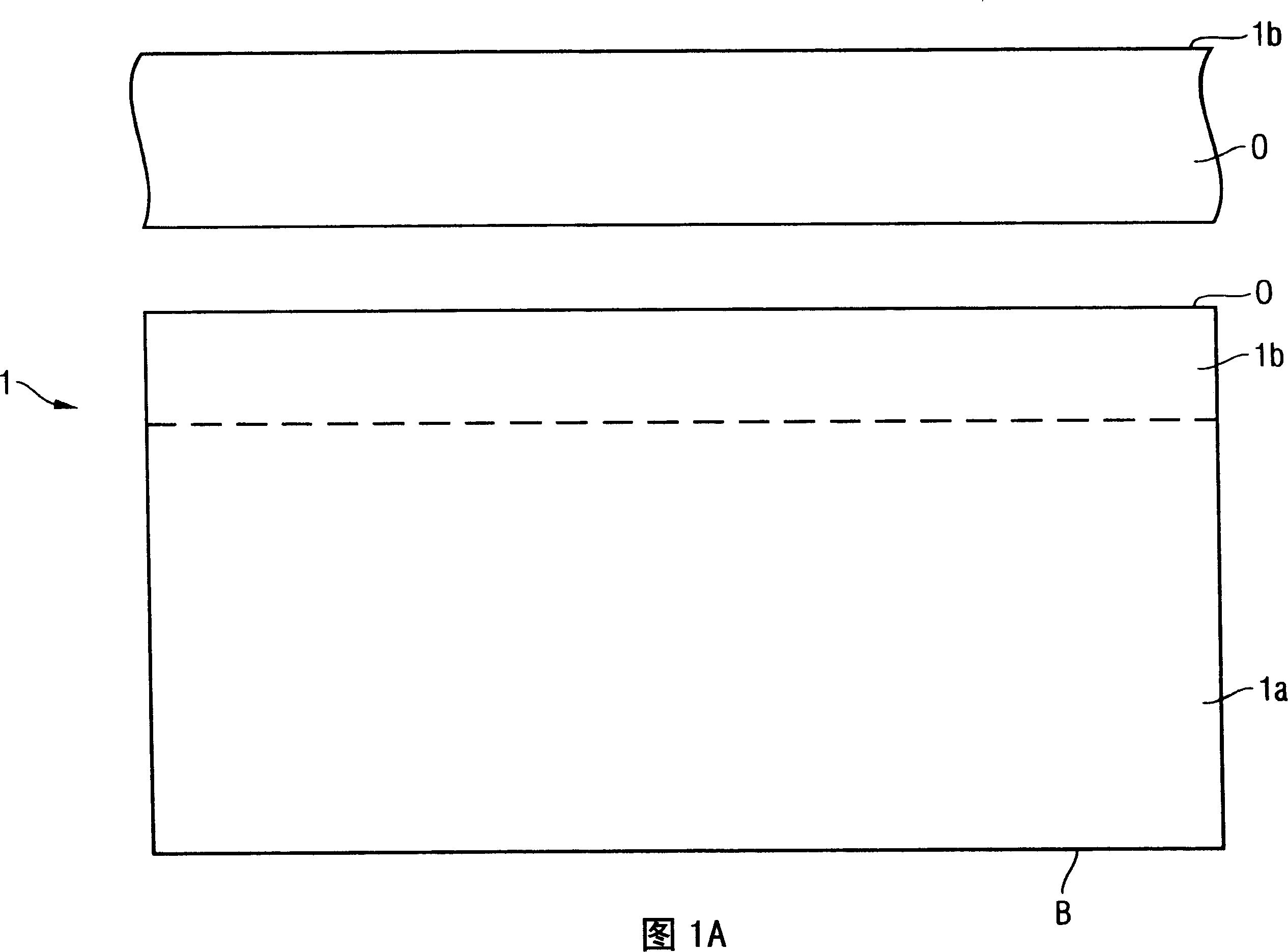
[0023] In FIG. 1A, reference numeral 1 denotes a silicon semiconductor wafer. A typical thickness of the silicon semiconductor wafer 1 is between 100 and 760 μm. A silicon semiconductor wafer 1 comprises a body region 1a on the wafer backside B and an active region 1b on the wafer front side 0, where integrated circuit elements (eg memory cells and peripheral devices) are to be formed. In the upper part of Fig. 1A, a partial view of the upper surface 0 of the active region 1b is shown.

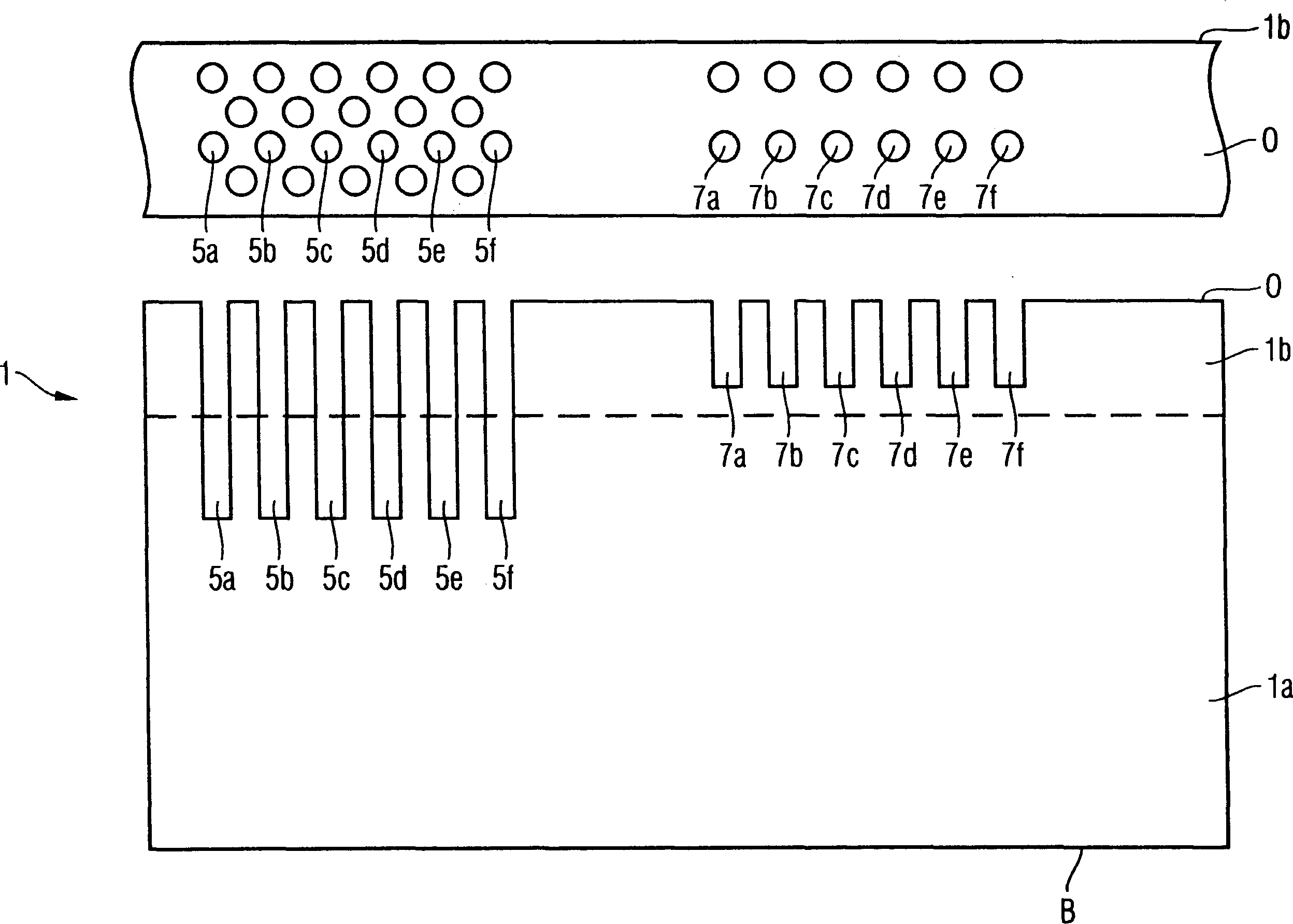
[0024] exist Figure 1B In the next process step shown in , storage capacitor trenches 7a-7f are formed in the active region 1b, and a plurality of contact trenches 5a-5f are formed in the active region 1b, wherein the contact trenches 5a-5f extend into Body region 1a. A typical depth of the storage capacitor trenches 7a-7f is 5 to 10 μm and a typical depth of the contact trenches 5a-5f is 15 to 30 m. The trenches 5a-5f may be formed in two successive process steps using the well-known anis...


PUM


Abstract

The invention provides a method of manufacturing a semiconductor structure having a wafer through-contact that can be achieved easily and safely. The method of manufacturing a semiconductor structure having a wafer through-contact comprises: a step of providing a semiconductor wafer (1) having a bulk region (1a) and an active region (1b); a step of forming multiple contact trenches (5a-5f), which extend from the top surface (0) of the active region (1b) to the bulk region (1a), in the semiconductor wafer (1); a step of forming a first dielectric isolation layer (8) on the sidewalls and the bottoms of the contact trenches (5a-5f); a step of providing a first conductive filler (10) in the multiple contact trenches (5a-5f); a step of forming a via (V) that is arranged in the semiconductor wafer (1), extends from the backside (B) of the bulk region (1a) to the multiple contact trenches (5a-5f), and exposes the conductive filler (10); a step of forming a second dielectric isolation layer (15) on the sidewall of the via (V); and a step of providing a second conductive filler (20) in the via (V) which comes into contact with the exposed conductive filler (10).

Description

technical field [0001] The present invention relates to a method of manufacturing a semiconductor structure with a through-contact in a wafer, and a corresponding semiconductor structure. Background technique [0002] Typically, vias are formed on the wafer front side in aluminum pads, and the metal (copper (Cu), nickel (Ni), tin (Sn), etc.) or metal alloy (tin Subsequent galvanic or non-galvanic deposition (electroplating or electroless deposition) of lead (SnPb, tin-silver (SnAg), etc.) to provide through-contacts in silicon wafers (i.e., contacts interconnecting the backside of the wafer with the frontside ). These vias are typically provided using wet chemical etching (eg, KOH) or dry chemical etching. The sidewalls of the vias are passivated (eg, by oxidation) and coated with a thin layer of metal (sputtering, MOCVD, etc.) prior to filling. The galvanic or non-galvanic processes are relatively complex and expensive because of the relatively large volumes that must be...

Claims


Application Information

Patent Timeline
Patent Type & Authority Applications(China)
IPC IPC(8): H01L21/768H01L23/522
CPCH01L21/76898
Inventor 哈里·海德勒罗兰·依尔西格勒
Owner QIMONDA
Why Eureka
Try Eureka