Information processing device

一种信息处理设备、平面显示器的技术,应用在电数字数据处理、数字输出到显示设备、数据处理的输入/输出过程等方向,能够解决相移信号波形模糊、显示不精确、写周期变短等问题

Inactive Publication Date: 2007-02-14
SEMICON ENERGY LAB CO LTD
View PDF6 Cites 2 Cited by
  • Summary
  • Abstract
  • Description
  • Claims
  • Application Information

AI Technical Summary

Problems solved by technology

[0013] When an image signal with a very fast dot clock is to be processed, the write cycle of the image signal to the display pixel becomes shorter, and in conventional TFTs, many problems will occur, such as phase shift, noise, signal waveform blurring etc., the display becomes imprecise

Method used


Image

  • Information processing device
  • Information processing device
  • Information processing device

Examples


Embodiment 1

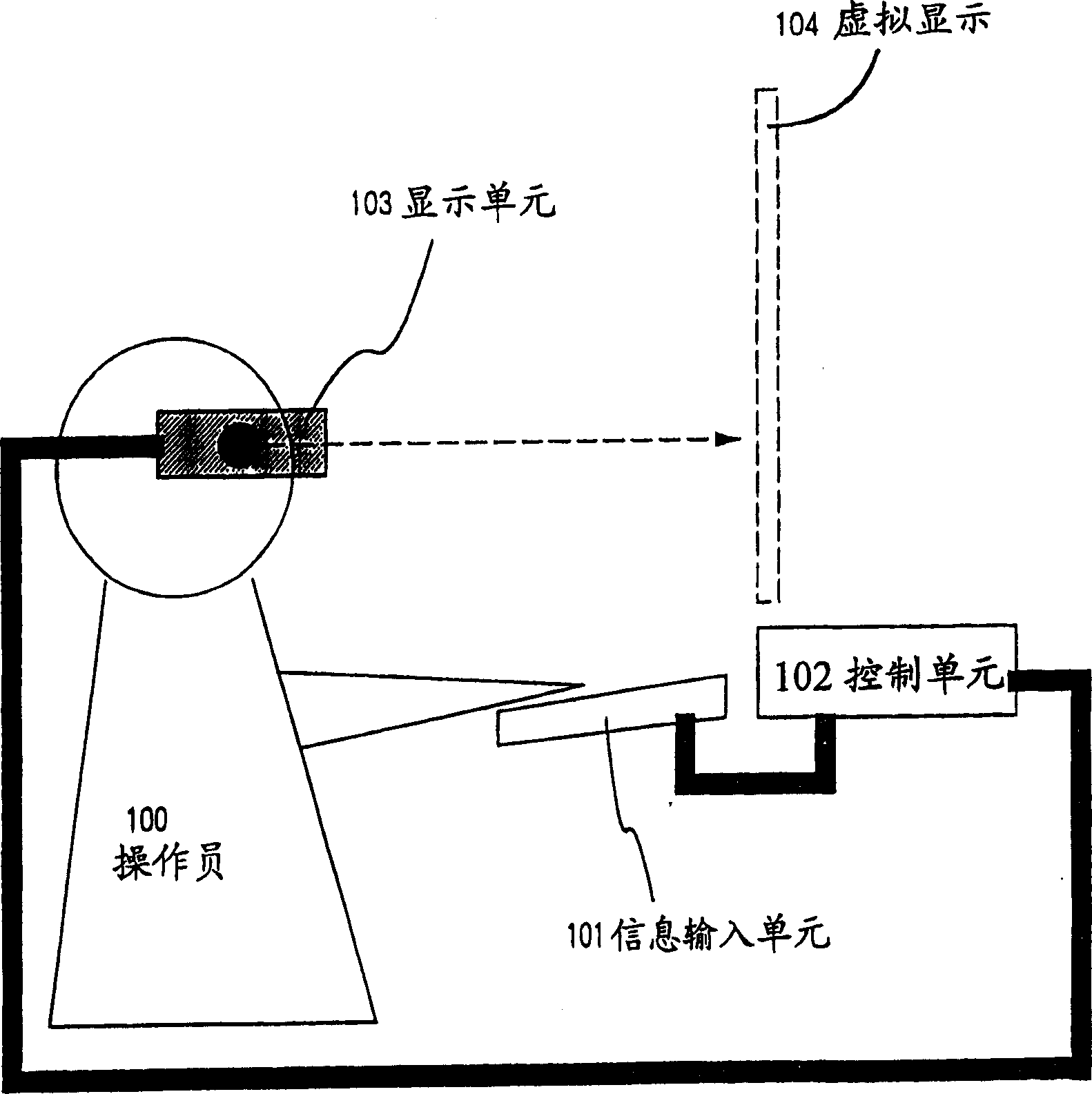
[0064] figure 1 is a schematic diagram of the information processing device of this embodiment. figure 2 is the external shape of the display unit (head-mounted display) shown in this embodiment. As a display method in this embodiment, a 2D (plane) image is displayed.

[0065] like figure 1 As shown, the display unit 103 is electrically connected to the input terminal unit 101 and the control unit 102 (computer, etc.). These three constitute an information processing device and system.

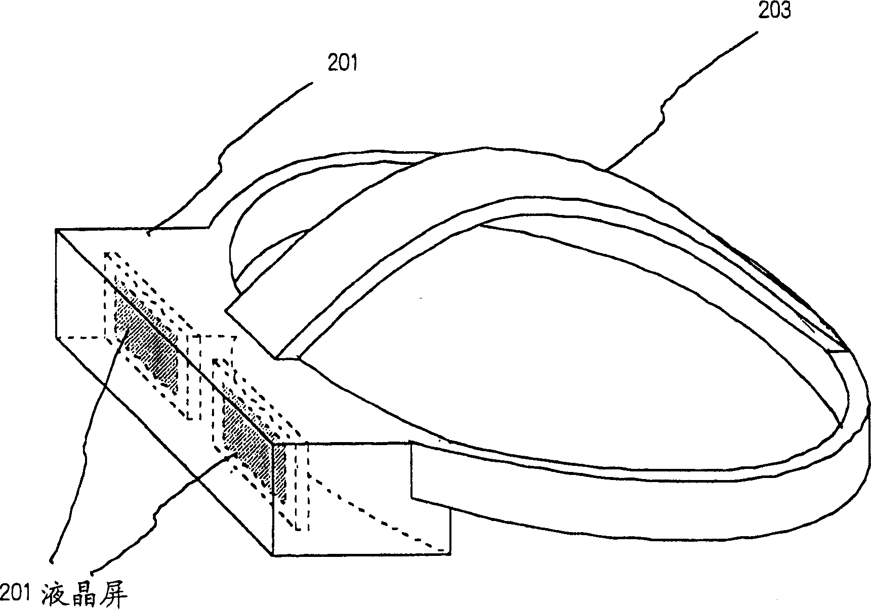
[0066] figure 2 The display unit shown in has a strap 203 for fixing a main body 201 in front of the user's eyes and a small active matrix type liquid crystal panel 202 of 0.2 to 2.6 inches for displaying images. In this embodiment, a small LCD screen of 1.4 inches is used. The strap 203 may also be replaced by any device that can be used to secure the main body in front of the user's eyes. For example, a frame structure like an eye frame can be used.

[0067] Among the liquid crysta...

Embodiment 2

[0088] This embodiment shows an example of virtually displaying 3D (three-dimensional image) images using a display unit (head-fixed display). Refer below Figure 4 This embodiment will be described. The liquid crystal panel of the display device is characterized in that the semiconductor thin film of the switching element is formed of continuous grain boundary crystalline silicon (CGS), realizes row-sequential scanning of pixel TFTs, and operates in a frequency range that cannot be recognized by the human eye (approximately 45Hz to 180Hz) to achieve AC drive.

[0089] For a 3D (three-dimensional image) image, two different image information, namely, an image signal 406 for the right eye and an image signal 407 for the left eye are prepared. In this embodiment, two different image signals are formed by an external unit (control unit, storage unit, etc.) and input to the LCD screen for the right eye and the LCD screen for the left eye respectively, thereby simplifying the dis...

Embodiment 3

[0094] In this embodiment, an example of manufacturing steps in which an active matrix region and a peripheral driver circuit are integrated on a glass substrate or a quartz substrate and a liquid crystal panel is manufactured will be described with reference to FIGS. 5A to 5E. Applying the fabrication steps shown in this example, one can obtain Figures 2 to 4 LCD screen shown.

[0095] First, as shown in FIG. 5A, a silicon oxide film 502 having a thickness of 3000 Å is formed as a base film on an insulating substrate 501 by a sputtering method.

[0096] Next, an amorphous silicon film was formed to a thickness of 400A by the low-pressure CVD method, which is not shown in the figure. This amorphous silicon film is crystallized to obtain a crystalline silicon film called continuous grain silicon (CGS). This crystalline silicon film configuration is formed into patterns 503, 504, and 505 in FIG. 5A. A method for producing such a crystalline silicon film called CGS will be de...


PUM


Abstract

An information processing device and its system is provided in which a head mounted display is used and a user carries out an information processing operation while seeing a virtual display screen. Polycrystalline silicon using CGS is used for a semiconductor of a display element of a liquid crystal panel used in the head mounted display, so that high speed driving is made possible. The display unit which frame reversal (60 to 180 Hz) is finished in a writing period is connected to a control unit and an input operating unit, so that the user can carry out the information processing operation.

Description

[0001] The application for the present invention is a divisional application of the patent application with the same title filed on February 9, 1999 and with application number 03157982.5. technical field [0002] The present invention relates to a display unit called a head mount display, which is fixed on the head and projects an image in front of the eyes, and to an information processing device using such a display unit and system. Background technique [0003] Generally, a user who handles electronic information realizes information processing operations by using a device as shown in FIG. 13 , which is a schematic diagram of the information processing device. In the specification of the present invention, an information processing operation means performing input, acquisition, transmission, exchange, storage, classification, etc. of information using a computer or the like. [0004] The input terminal unit 11 is a device for a user to perform an information input opera...

Claims


Application Information

Patent Timeline
Patent Type & Authority Applications(China)
IPC IPC(8): G02B27/01G06F3/00G02F1/13G06F3/01G06F3/048G06F3/0481
CPCG02B27/017G06F3/011G06F3/14
Inventor 山崎舜平平形吉晴西毅桑原秀明
Owner SEMICON ENERGY LAB CO LTD
Why Eureka
Try Eureka