Apparatus for processing substrate and apparatus for processing electron source substrate
A substrate processing device and electron source technology, applied to circuits, discharge tubes, electrical components, etc., can solve problems such as fluctuations in the concentration of organic compounds, slow formation of carbon films, and degradation of electron source uniformity
- Summary
- Abstract
- Description
- Claims
- Application Information
AI Technical Summary
Problems solved by technology
Method used
Image

Examples
example 1
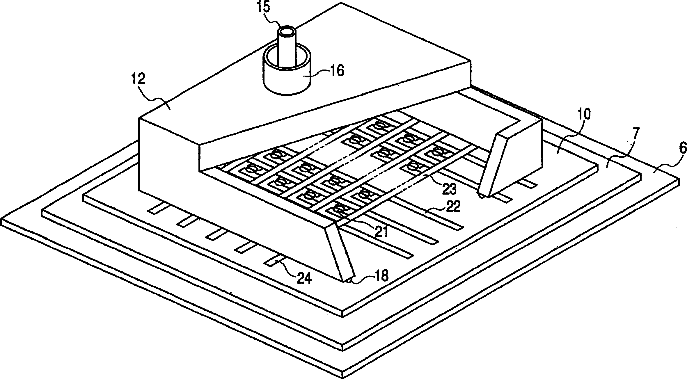
[0045] This example is used to make Figure 5 The electron source substrate shown, which has such Figure 4 Multiple surface conduction electron-emitting devices are shown. exist Figure 4 and 5 In , an electron source substrate 10, a conductive film 21, an X-direction wiring 22, a Y-direction wiring 23, a device electrode 25, a carbon film 26, a void 27 in the carbon film 26, and an insulating layer 28 are shown. For simplification purposes, Figure 5 The carbon film 26 is omitted.
[0046] First, on loaded SiO 2 A Pt paste was printed on the glass substrate and fired under heating conditions to form the device electrodes 25 . Ag paste was then screen-printed and fired under heating to form X-direction wiring 22 (240 wirings) and Y-direction wiring 23 (720 wirings). In the intersecting portion of the X-direction wiring 22 and the Y-direction wiring 23 , an insulating paste is screen-printed and fired under heating to form an insulating layer 28 .
[0047] Then, betwee...
example 2
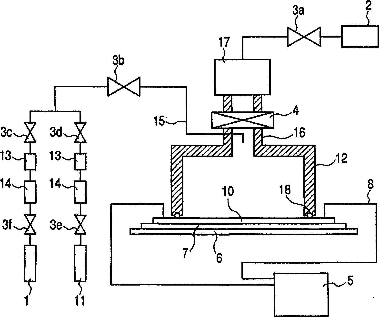
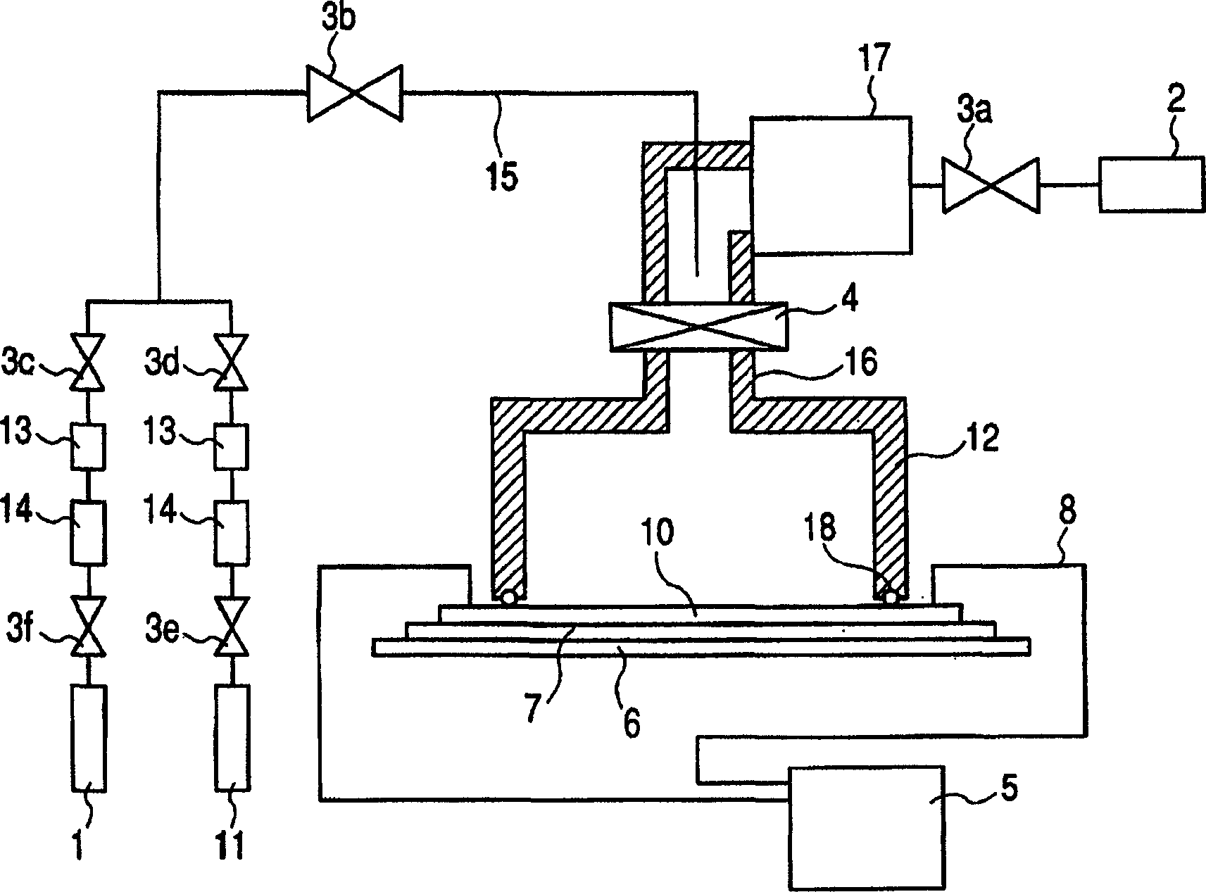
[0057] use image 3 The processing device shown was prepared in a manner similar to Example 1 Figure 5 An electron source substrate 10 is shown. In this example, the introduction port of the gas introduction pipe 15 is made vertically movable within the exhaust pipe 16 by a driving mechanism not shown. In the activation process, the introduction port of the gas introduction pipe 15 is lowered by the driving mechanism to a position lower than the gate valve 4 and closer to the substrate 10 in the exhaust pipe 16 . A mixed gas of the organic compound gas 11 and the carrier gas 1 is introduced into the sealed container 12 by opening the gas supply valves 3c, 3d, and 3b. Nitrogen gas mixed with ethylene was used as the organic compound gas 11, and nitrogen gas was used as the carrier gas 1. According to airtight container 12 with 1.3 x 10 -4 The opening degree of the valve 3b is adjusted by means of the internal pressure of Pa, under the monitoring of an unillustrated vacuum ...
example 3
[0061] This example shows the application of the substrate processing apparatus of the present invention to a plasma processing apparatus. Figure 6 The configuration of the apparatus of this example is shown, in which a high-frequency oscillator 30, a substrate 31, a sealed container 32, a plasma processing chamber 33, an exhaust pipe 34, a gate valve 35, a vacuum pump 36, a gas introduction pipe 37, high Frequency introduction window 38 and waveguide 39.
[0062] In this example, a plasma processing chamber 33 is disposed within a sealed container 32 . A substrate 31 to be processed is located in a processing chamber 33 which is connected to an exhaust pipe 34 and evacuated by means of a vacuum pump 36 . A gas introduction pipe 37 is provided in the exhaust pipe 34 to supply process gas to the plasma processing chamber 33 . The high frequency oscillator 30 transmits high frequency waves to the plasma processing chamber 33 through the waveguide 39 and the high frequency int...
PUM
 Abstract
Description
Claims
Application Information
 - R&D
- Intellectual Property
- Life Sciences
- Materials
- Tech Scout
- Unparalleled Data Quality
- Higher Quality Content
- 60% Fewer Hallucinations
Browse by: Latest US Patents, China's latest patents, Technical Efficacy Thesaurus, Application Domain, Technology Topic, Popular Technical Reports.
© 2025 PatSnap. All rights reserved.Legal|Privacy policy|Modern Slavery Act Transparency Statement|Sitemap|About US| Contact US: help@patsnap.com