
Liquid crystal display drive circuit

A liquid crystal driving circuit and driving voltage technology, applied in the direction of logic circuit connection/interface layout, optics, instruments, etc., can solve the problems of large through current or charging and discharging current, driving voltage and voltage fluctuation, and chip size influence, etc. Prevents shoot-through current from flowing through the output transistors, reduces the number, and realizes the effect of power consumption

Inactive Publication Date: 2007-02-28
SANYO ELECTRIC CO LTD
View PDF1 Cites 0 Cited by
  • Summary
  • Abstract
  • Description
  • Claims
  • Application Information

AI Technical Summary

Problems solved by technology

[0009] However, the existing liquid crystal drive circuit is composed of two NAND circuits (the first and the second NAND circuits 50, 51) and two NOR circuits (the first and the second NOR circuits 52, 53), and the on-off control of the output transistor is performed. Therefore, the number of transistors in the output control circuit part is up to 16
Therefore, there is a problem that the chip size of the LSI of the driving circuit becomes larger
In particular, since the driving voltage is a high voltage of 30V to 40V, not only the output transistors, but also the transistors constituting the NAND circuit or the NOR circuit also need to be designed with high withstand voltage transistors that occupy a large area. The increase in the number of transistors brings a large impact on the chip size. Impact
[0010] In addition, with the transition of the dot signal DA and the field signal DF (transition from low to high or from high to low), the through current or charge and discharge current of the NAND circuit or NOR circuit and the output transistor becomes very large, resulting in Increase in power consumption and voltage fluctuations in drive voltage

Method used


Image

  • Liquid crystal display drive circuit
  • Liquid crystal display drive circuit
  • Liquid crystal display drive circuit

Examples


Embodiment Construction

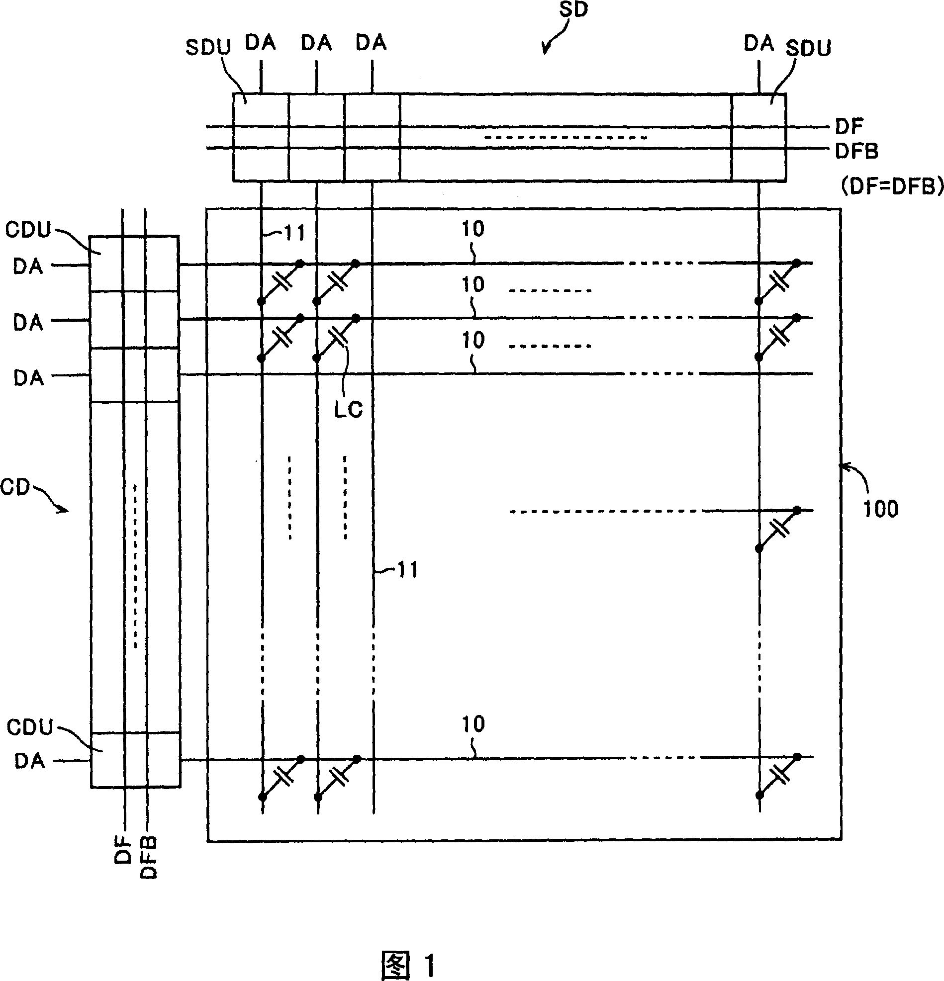
[0022] Next, embodiments of the present invention will be described with reference to the drawings. FIG. 1 is a diagram showing the structure of a dot matrix type STN-LCD panel. In this STN-LCD panel, a common driver CD and a segment driver SD are provided around the display area 100 . The common driver CD has a plurality of common drivers / units CDU with the same circuit structure. In each driver / unit CDU, a dot signal DA, a field signal DF common to each driver / unit CDU, and an inverted field signal DFB are supplied. The segment driver SD also has a plurality of segment drivers / units SDU with the same circuit configuration, but the field signal DF and the inverted field signal DFB are set to the same signal.

[0023] Output signals of the driver / unit CDU are output to corresponding row lines 10 , and output signals of the segment driver / unit SDU are output to corresponding column lines 11 . A liquid crystal capacitor LC is formed at each intersection of the row line 10 and...


PUM


Abstract

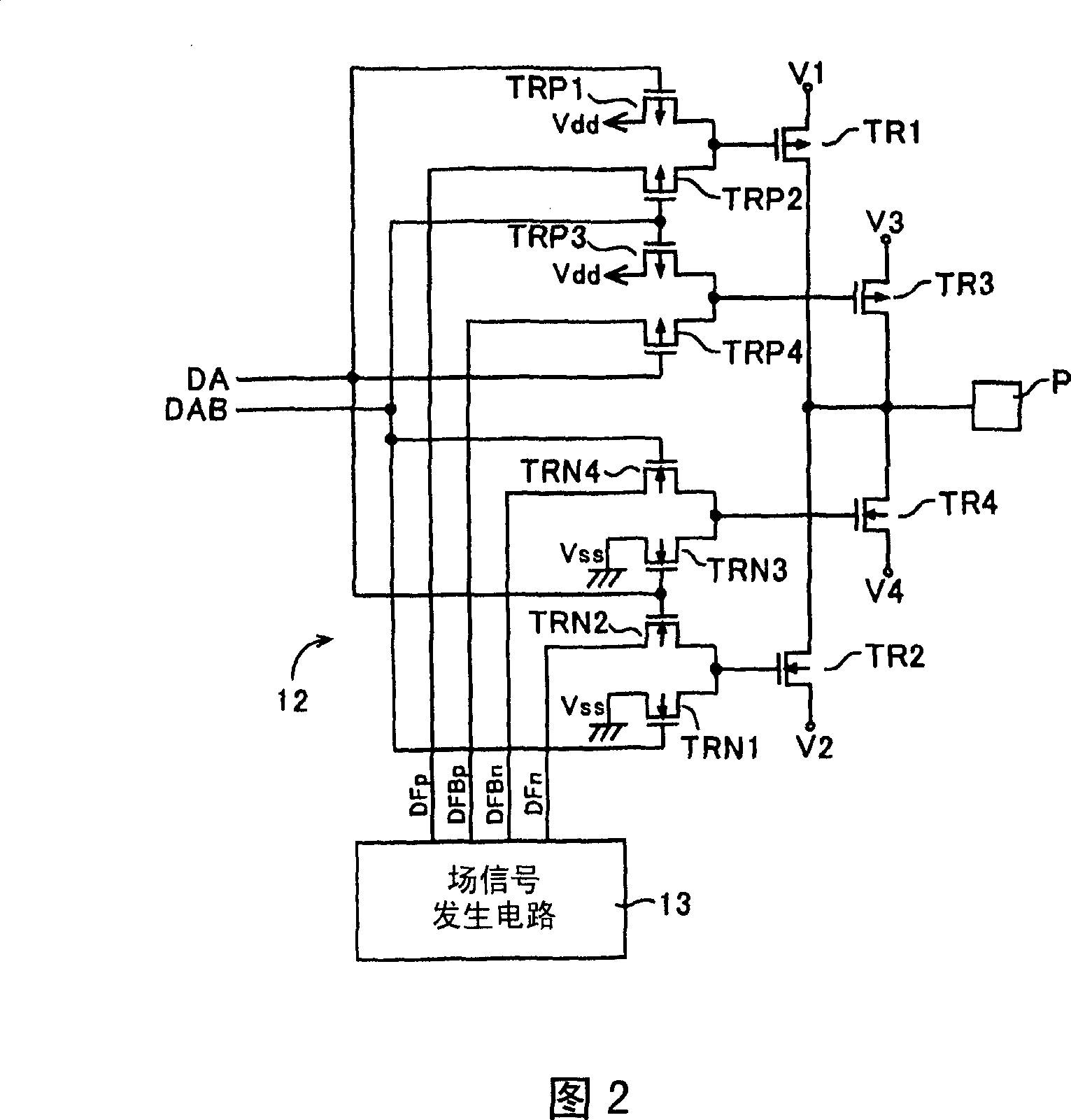
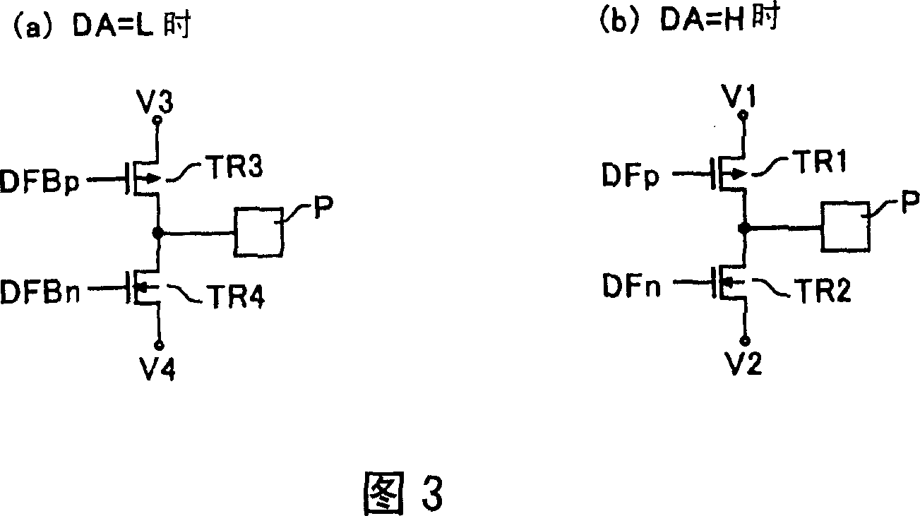
In the liquid crystal drive circuit of the present invention, each of the four output transistors ( TR1 to TR4 ) is provided with two control transistors for each output transistor, for a total of eight control transistors. According to the dot signal (DA) and the field signal (DF), the eight control transistors are turned on and off, and one output transistor is selected from the four output transistors ( TR1 to TR4 ). By sharpening the rising edges of (DFp, DFBp) and the falling edges of (DFn, DFBn) applied to the output transistors ( TR1 to TR4 ), the output transistors are shifted from on to off earlier. Further, by slowing the falling edge of (DFp, DFBp) and the rising edge of (DFn, DFBn), each output transistor is delayed from OFF to ON. Therefore, in the liquid crystal drive circuit, the number of transistors in the output control circuit is greatly reduced, and the power consumption is reduced and the drive voltage is stabilized.

Description

technical field [0001] The invention relates to a liquid crystal drive circuit, in particular to a drive circuit for an STN-LCD panel (STN-LCD is a super twisted nematic liquid crystal). Background technique [0002] Generally speaking, the driving circuits for STN-LCD panels are divided into two types: common driver and segment driver. The common driver and the segment driver output multi-bit driving signals to corresponding data lines (row lines or column lines), and each bit has 4 output transistors. By turning on one of these output transistors, the other The output transistor is turned off, and the drive voltage of any one of the four drive voltages V1, V2, V3, and V4 is output. A liquid crystal capacitor is formed at the intersection of the row line and the column line, and the liquid crystal display of dot matrix is ​​performed by applying the driving voltage to the liquid crystal capacitor. [0003] FIG. 4 is a circuit diagram showing a one-bit output control circu...

Claims


Application Information

Patent Timeline
Patent Type & Authority Applications(China)
IPC IPC(8): G09G3/36G09G3/20G02F1/133
CPCG09G3/3692G09G3/3681G09G2330/021G09G3/36G02F1/133G09G3/20H03K19/0175
Inventor 山濑真也
Owner SANYO ELECTRIC CO LTD
Learn More