Production of flash memory

A manufacturing method and memory technology, which is applied in semiconductor/solid-state device manufacturing, electrical components, circuits, etc., can solve problems such as improving the integration of components, and achieve the effects of reduced contact resistance, small size, and large process space

Inactive Publication Date: 2007-04-04
POWERCHIP SEMICON CORP
View PDF0 Cites 1 Cited by
  • Summary
  • Abstract
  • Description
  • Claims
  • Application Information

AI Technical Summary

Problems solved by technology

[0008] In view of this, the object of the present invention is to propose a method for manufacturing flash memory to solve the problems arising from the improvement of component integration

Method used


Image

  • Production of flash memory
  • Production of flash memory
  • Production of flash memory

Examples


no. 1 example

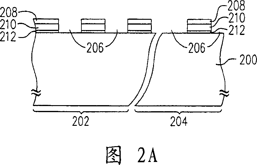
[0100] FIG. 2A to FIG. 2F illustrate a manufacturing flow chart of a flash memory according to a preferred embodiment of the present invention. Wherein, FIG. 2E and FIG. 2F belong to the same manufacturing process step, and FIG. 2E is a cross-sectional view along the section line I-I' and section line II-II' of FIG. 2D. FIG. 2F is a subsequent manufacturing flow chart of FIG. 2E .

[0101] Referring to FIG. 2A , firstly, a substrate 200 is provided. The substrate 200 can be divided into a memory cell area 202 and a peripheral circuit area 204 . Next, a dielectric material layer (not shown), a conductive material layer (not shown), and a mask layer (not shown) are sequentially formed on the substrate 200 . The material of the dielectric material layer is, for example, silicon oxide, and its formation method is, for example, thermal oxidation. The material of the conductor material layer is, for example, doped polysilicon, and its formation method is, for example, chemical va...

no. 2 example

[0114] FIG. 3A to FIG. 3E illustrate a manufacturing flow chart of a flash memory according to a preferred embodiment of the present invention. Wherein, FIG. 3C and FIG. 3D belong to the same manufacturing process step, and FIG. 3D is a cross-sectional view drawn along the section line I-I' and section line II-II' of FIG. 3C. FIG. 3E is a subsequent manufacturing flow chart of FIG. 3D .

[0115] Referring to FIG. 3A , firstly, a substrate 300 is provided. The substrate 300 can be divided into a memory cell area 302 and a peripheral circuit area 304 . A plurality of device isolation structures 306 have been formed in the substrate 300 . A dielectric layer 308 and a conductive layer 310 disposed on the dielectric layer 308 are formed between two adjacent device isolation structures 306 in the memory cell area 302 . A dielectric layer 312 is formed between two adjacent device isolation structures 306 in the peripheral circuit area 304 , and a conductive layer 314 is formed on ...


PUM


Abstract

A production method using for flash memory offers basement with location and peripheral circuit. The basement has designed dielectric layer and the first conductor layer and uses picture of the said dielectric layer and the first conductor layer to form some insulation structure of component inside the basement. Form dielectric layer of bars and thin polycrystalline silicon layer on basement in turn and remove the thin polycrystalline silicon layer and dielectric layer of bars of the peripheral circuit. After forming the second dielectric layer and mask on basement, design each of layer and form location inside the location area and grid structure inside the peripheral circuit. Form electric pin connecting with the second conductor layer on grid structure. For the dielectric layer of bars to peripheral circuit having been removed, the electric pin formed on the peripheral circuit saves technology and enhances margin of technology.

Description

technical field [0001] The invention relates to a manufacturing method of a semiconductor element, in particular to a manufacturing method of a flash memory. Background technique [0002] Memory is a semiconductor device used to store data or data. When the functions of computer microprocessors become stronger and stronger, and the programs and calculations performed by software become larger and larger, the demand for memory becomes higher and higher. In order to manufacture large-capacity and cheap memory to meet this demand, the technology and process of making memory components has become the driving force for semiconductor technology to continue to challenge high integration. [0003] Flash memory (Flash Memory) components have the advantages of being able to store, read, and erase data multiple times, and the stored data will not disappear after power failure, so it has become a popular choice for personal computers and electronic devices. A non-volatile memory eleme...

Claims


Application Information

Patent Timeline
Patent Type & Authority Applications(China)
IPC IPC(8): H01L21/8239H01L21/8246H01L21/768
Inventor 刘思贤魏鸿基
Owner POWERCHIP SEMICON CORP
Why Eureka
Try Eureka