Structure for avalanche improvement of ultra high density trench mosfet

A technology of grooves and substrates, applied in the direction of electrical components, electrical solid devices, circuits, etc., can solve the problem of increasing unit density

Inactive Publication Date: 2007-04-04
谢福渊
View PDF0 Cites 33 Cited by
  • Summary
  • Abstract
  • Description
  • Claims
  • Application Information

AI Technical Summary

Problems solved by technology

Therefore, for semiconductor devices such as MOSFETs, it is still difficult to achi

Method used


Image

  • Structure for avalanche improvement of ultra high density trench mosfet
  • Structure for avalanche improvement of ultra high density trench mosfet
  • Structure for avalanche improvement of ultra high density trench mosfet

Examples


Embodiment Construction

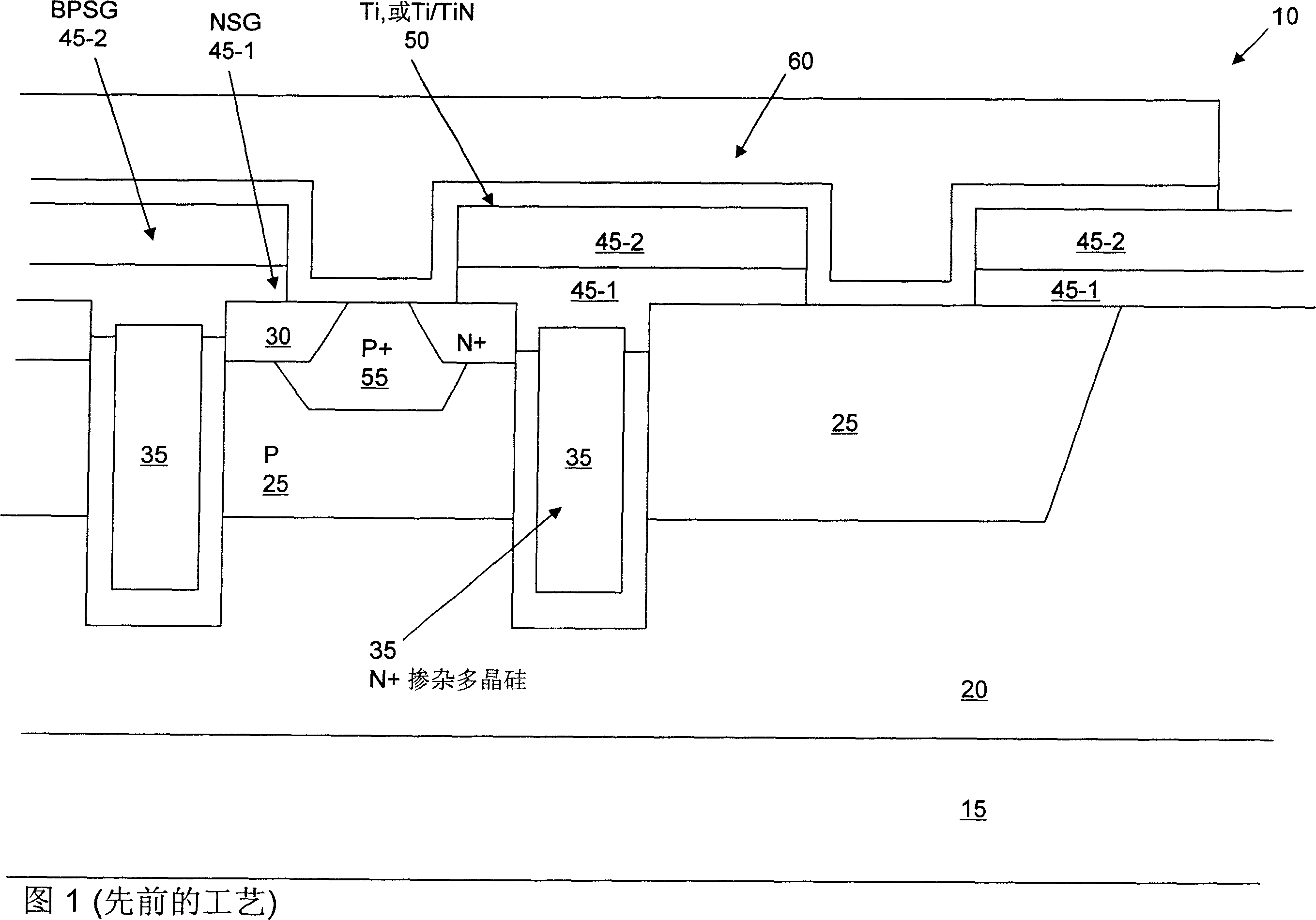
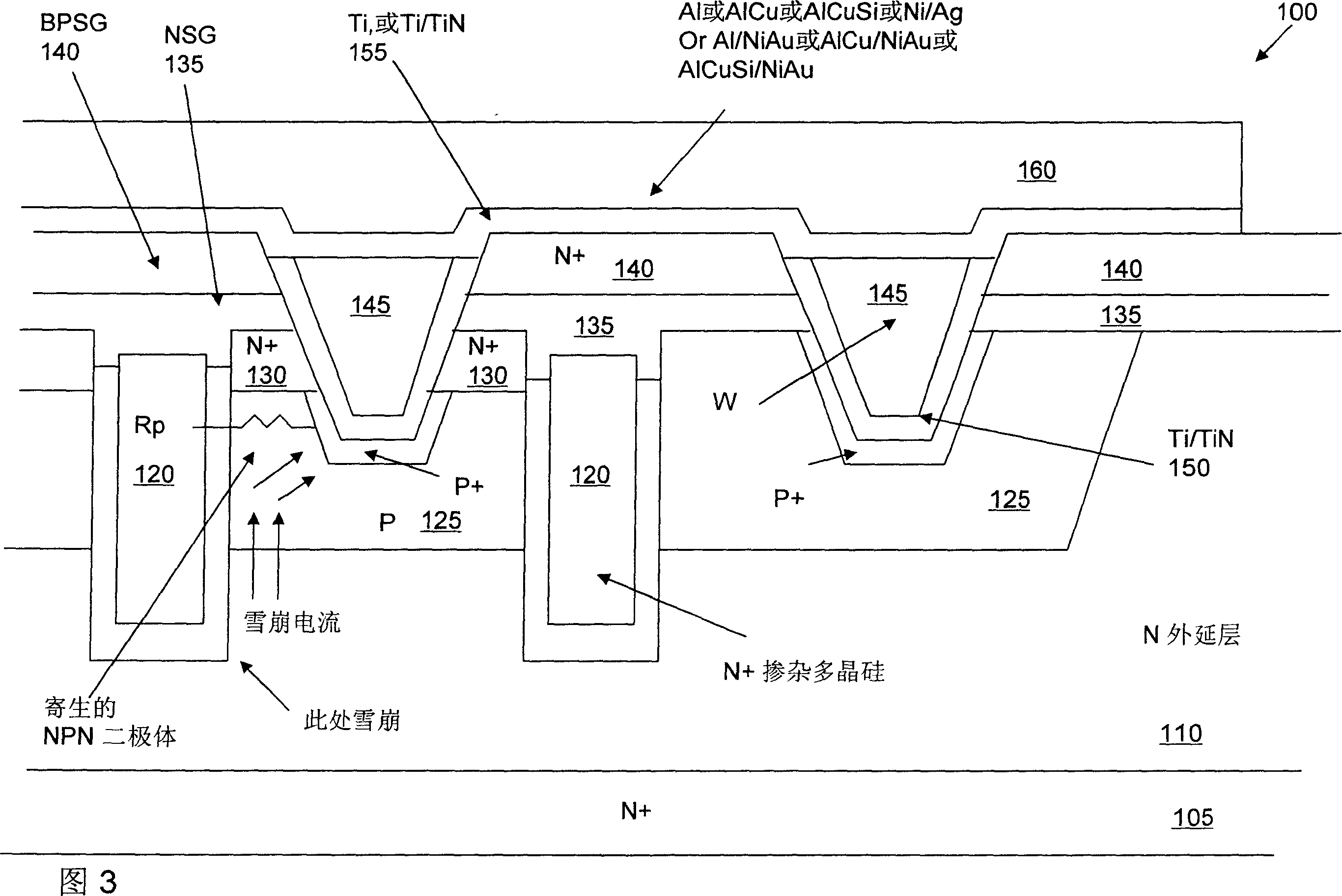
[0023] FIG. 3 shows the first recommended solution of the present invention, in which a metal oxide semiconductor field effect transistor (MOSFET) device 100 is mounted on an N+ substrate 105 formed with an N epitaxial layer 110. The MOSFET device 100 includes a trench gate 120, which is disposed in a trench with a gate insulating layer 115 formed on the wall. A base region 125 doped with impurities of the second conductivity type, such as P-type impurities, extends between the trench gates 120. The P-base region 125 surrounds a source region 130 doped with impurities of the first conductivity type, for example, N+ impurities. The source region 130 is formed near the top surface of the epitaxial layer surrounding the trench gates 125 (may be 120). Extending on the upper surface of the semiconductor substrate above the trench gate, the base region 125 and the source region 130 are respectively covered by an undoped silicon glass (NSG) and a borophosphosilicate glass BPSG protective...


PUM


Abstract

A trench metal-oxide-semiconductor field-effect transistor (MOSFET) cell having a trenched gate surrounded by a source region between a body region disposed above a drain on the bottom surface of a substrate Inside. The MOSFET cell also has a source-body contact trench opened such that its sidewalls extend substantially perpendicular to the upper surface into the source and body region and are filled with contact metal plugs. forming a body-resistance reducing region doped with a body impurity to surround the source-body contact trench to reduce the body-region resistance between the source-body contact metal and the trench gate to improve avalanche ability.

Description

Technical field [0001] The present invention generally relates to the unit structure and manufacturing process of power semiconductor devices. In more detail, the present invention will introduce a new and improved cell structure and an improved manufacturing method for trench semiconductor power devices with improved avalanche capability. Background technique [0002] The traditional process of forming aluminum metal contacts between the N+ source and the P-well formed in the P base region in a semiconductor device will encounter technical difficulties with poor metal coverage and unreliable electrical contacts when the cell pitch is reduced. When the metal oxide semiconductor field effect transistor (MOSFET) cell density increases to 200 million cells per square inch (200M / in 2 ) Above, the cell pitch is reduced to 1.8 microns or even smaller, this technical difficulty is particularly significant. For the case where the cell density exceeds 200 million cells per square inch, th...

Claims


Application Information

Patent Timeline
IPC IPC(8): H01L29/78
CPCH01L2924/01074H01L2924/13091
Inventor 谢福渊
Owner 谢福渊
Why Eureka
Try Eureka