TET LCD array substrate structure and its producing method

An array substrate structure and substrate technology, which is applied in semiconductor/solid-state device manufacturing, optics, instruments, etc., can solve problems such as the need to change the process manufacturing process, do not involve the improvement of storage capacitance, and reduce the capacitance of drain-source electrodes, so as to reduce the area, Improve display quality and improve the effect of storage capacitors

Active Publication Date: 2007-04-11
BEIJING BOE OPTOELECTRONCIS TECH CO LTD +1
View PDF3 Cites 19 Cited by
  • Summary
  • Abstract
  • Description
  • Claims
  • Application Information

AI Technical Summary

Problems solved by technology

However, the common disadvantage of the above structures is that the aperture ratio decreases.
US Patent No. 6,953,715 is mainly aimed at changing the insulating layer material to control the size of the storage capacitor. The advantage is that there is no change in the structure. The disadvantage is that the materials used and the manufacturing process need to be changed.
U.S. Patent No. 6,661,477 designed an island gate electrode, and at the same time connected the pixel electrode to the metal of the source electrode layer to reduce the capacitance of the drain-source electrode, so as to improve the poor crosstalk. Although the pixel electrode is also connected to the metal of the source electrode layer in structure, it is not Involved in the storage capacitor improvement part

Method used


Image

  • TET LCD array substrate structure and its producing method
  • TET LCD array substrate structure and its producing method
  • TET LCD array substrate structure and its producing method

Examples


Embodiment Construction

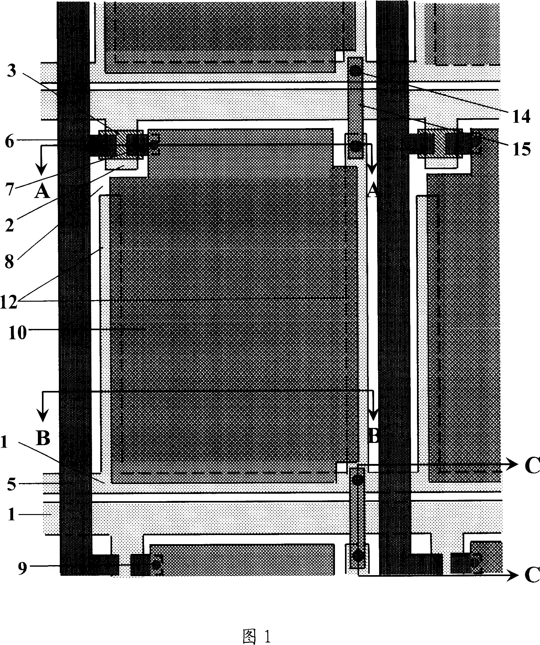
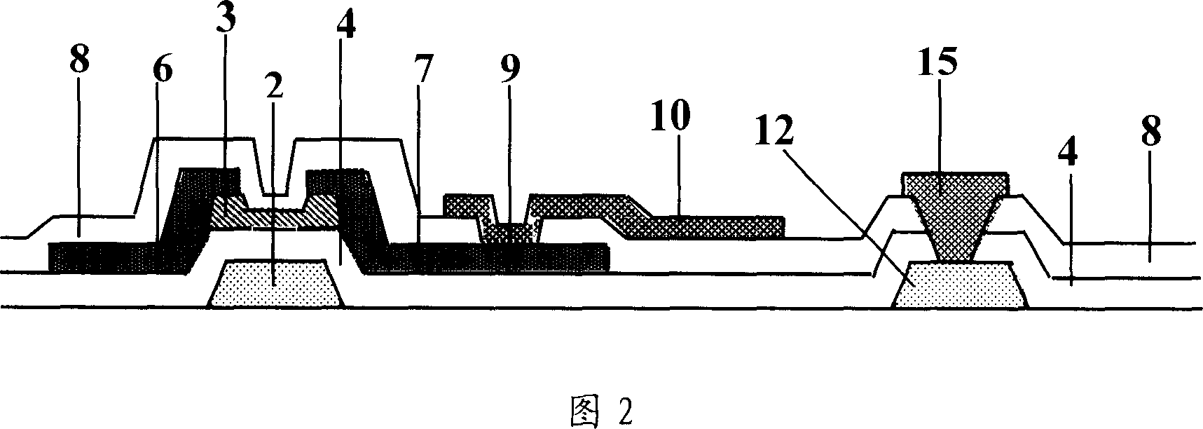
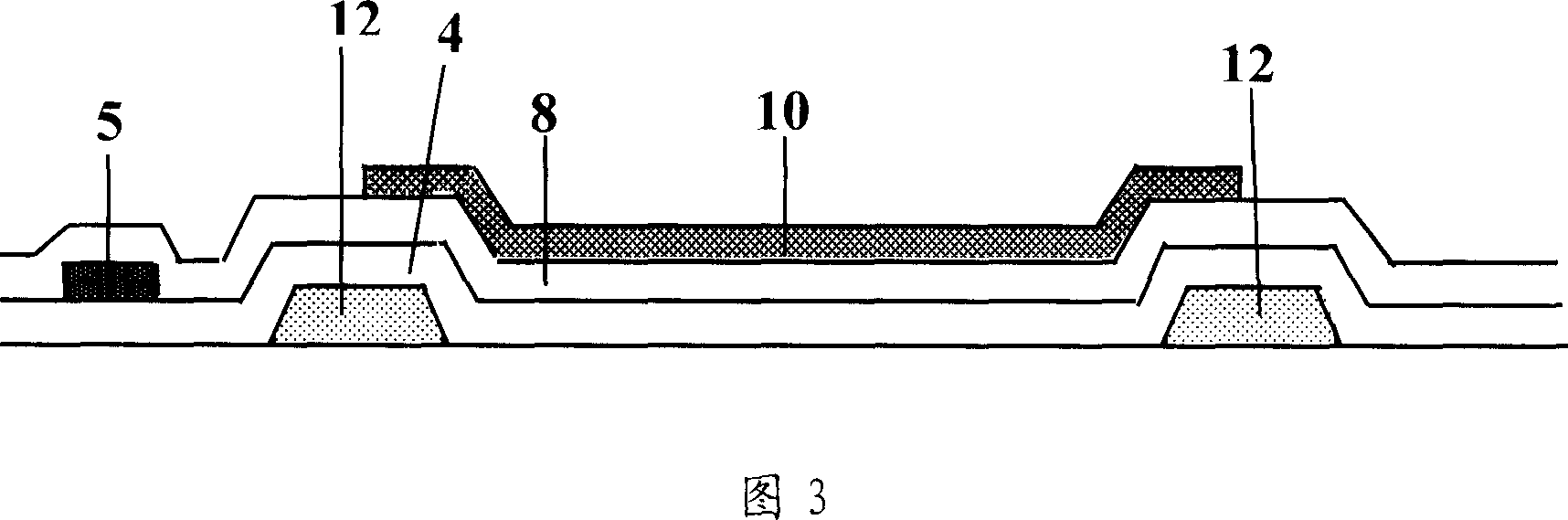
[0043]FIG. 6 is a top view of the structure of the TFT LCD array substrate of the present invention. As shown in Figures 6 to 9, on the TFT LCD array substrate there is a group of gate scanning lines 1 and common electrodes 13 parallel thereto, and a group of data scanning lines 5 perpendicular thereto, and adjacent gate scanning lines and data scanlines define the pixel area. Each pixel includes a TFT switch device, a transparent pixel electrode 10, two light-shielding strips 12 and part of the common electrode 13. The common electrode 13 and the light-shielding strip 12 are connected to form an integrated structure. The passivation layer via hole 14 of the electrode is connected through the transparent pixel lead 15 of the common electrode. The TFT device is composed of a gate electrode 2 , a gate electrode insulating layer 4 , an active layer 3 , and a source electrode 6 and a drain electrode 7 . The transparent pixel electrode 10 is connected to the drain electrode 7 of ...


PUM


Abstract

This invention discloses a TFT LCD array base plate structure including: a base plate, a grid, grid scanning lines and a public electrode, in which, the public electrode is a base electrode of the storage capacitance, a grid insulation layer, an active layer and a channel on it, a data scanning line, source and drain, a top electrode of the storage capacitor formed above the grid insulation layer, a passivation layer and its through hole or groove formed above the drain and the storage capacitor top electrode, pixel electrode formed on the passivation layer and connected with the drain and the top electrode of the storage capacitor via the passivation layer through hole or groove. This invention also discloses a manufacturing method for said array base plate structure, which can reduce the area of light strips and the overlapped area between the light strip and pixel electrode, the publick electrode and the transparent electrode so as to increase the open-end rate and storage capacitance.

Description

technical field [0001] The invention relates to a thin film transistor liquid crystal display (TFT LCD), in particular to a thin film transistor liquid crystal display array substrate structure and a manufacturing method thereof. Background technique [0002] TFT LCDs feature low power consumption, relatively low manufacturing costs, and no radiation, and currently dominate the flat panel display market. The matrix-type common electrode structure avoids cross-talk (Cross-Talk), flicker (Flicker) and horizontal white lines caused by electrode signal differences. However, although the structure of the matrix-type common electrode improves the signal uniformity, the structure has a loss in the aperture ratio of the pixel. The TFT LCD device storage capacitor is the main means to maintain the potential of the pixel electrode after the pixel scanning signal ends, and increasing the storage capacitor of the pixel uniformly can effectively improve the uniformity of the picture. I...

Claims


Application Information

Patent Timeline
Patent Type & Authority Applications(China)
IPC IPC(8): H01L27/12H01L23/522H01L21/84H01L21/768G02F1/136
Inventor 彭志龙龙春平朴云峰
Owner BEIJING BOE OPTOELECTRONCIS TECH CO LTD
Why Eureka
Try Eureka