

Offset current mode spectrograph for scan tunnel and microscope for scan tunnel
A technology of scanning tunneling and bias current, which is applied in the field of scanning tunneling microscopy, can solve the problems of small microscope bandwidth and difficulty in measuring time gain, and achieve the effects of increasing gain and bandwidth, increasing gain, and low parasitic capacitance
- Summary
- Abstract
- Description
- Claims
- Application Information
AI Technical Summary
Problems solved by technology
Method used
Image

Examples
Embodiment 1
[0022] Embodiment 1: A basic structure of bias current type scanning tunneling spectrometer
[0023] In this embodiment, the sample is fixed, and the relative position between the probe and the sample is adjusted by moving the probe.
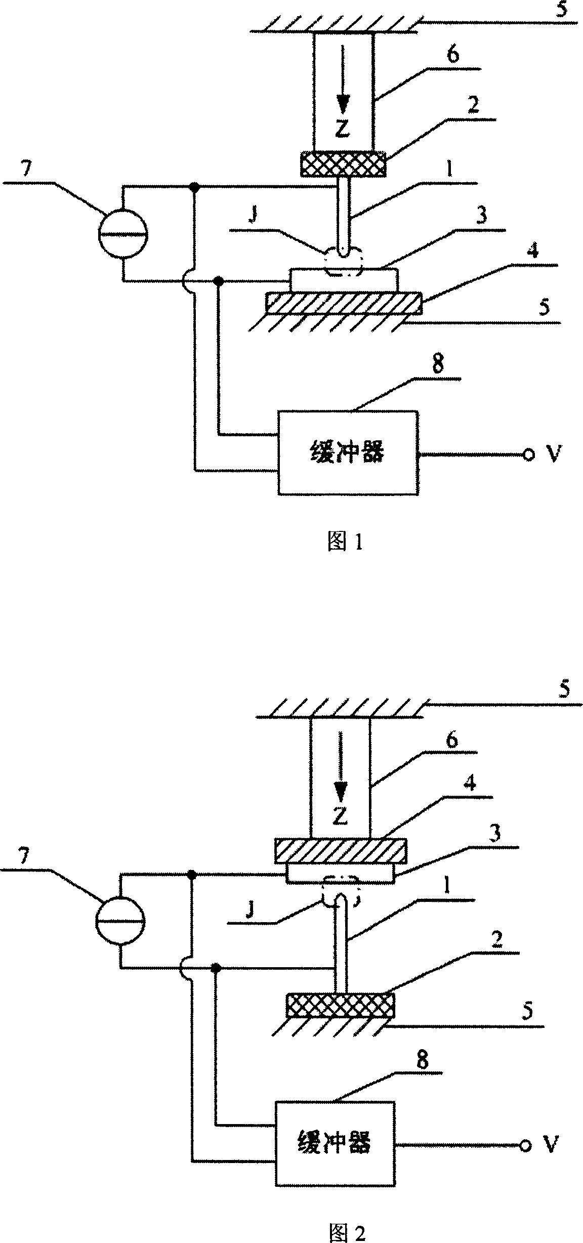
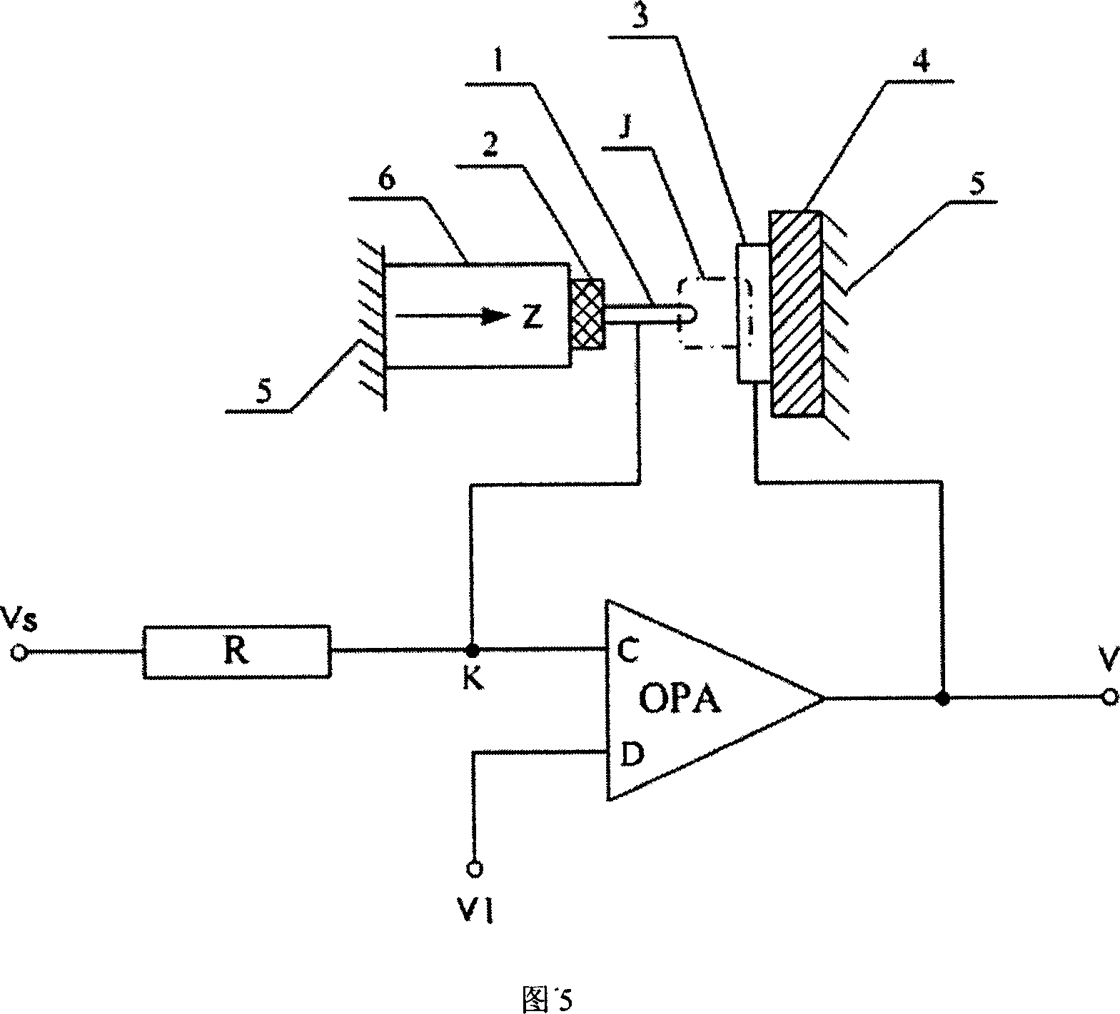
[0024]Figure 1 shows the schematic diagram of the structure and principle of the bias current scanning tunneling spectrometer in this embodiment: the sample 3 is fixed on the sample holder 4, the probe 1 is fixed on the probe holder 2, and the probe holder 2 is fixed on the Z position One end of the device 6, the sample holder 4 is fixed on the base 5, the other end of the Z positioner 6 is fixed on the base 5 or on another base with adjustable position so that the probe points to the sample on the sample holder , probe 1 and sample 3 form a tunnel junction J. The two poles of the current source 7 are respectively connected to the probe and the sample of the tunnel junction J through wires, and the polarity of the current source 7 can be revers...
Embodiment 2
[0027] Embodiment 2: another basic structure of bias current scanning tunneling spectrometer
[0028] The bias current scanning tunneling spectrometer in this embodiment adopts a fixed probe, and adjusts the relative position between the sample and the probe by moving the sample to obtain the voltage signal of the tunnel junction. Compared with Example 1, the positions of the probe-probe holder assembly and the sample-sample holder assembly of this embodiment are reversed.
[0029] Fig. 2 has provided the structure diagram of the bias current scanning tunneling spectrometer of this embodiment: the sample holder 4 is fixed on the top of the Z positioner 6, the sample 3 is fixed on the sample holder 4, and the probe 1 is fixed on the probe holder 2 , the probe holder 2 is fixed on the base 5, and the other end of the Z positioner 6 is fixed on the base 5 or another adjustable base so that the probe points to the sample on the sample holder. The current source 7 can be a DC curr...
Embodiment 3
[0031] Example 3: Bias current scanning tunneling microscope in equal-height scanning mode
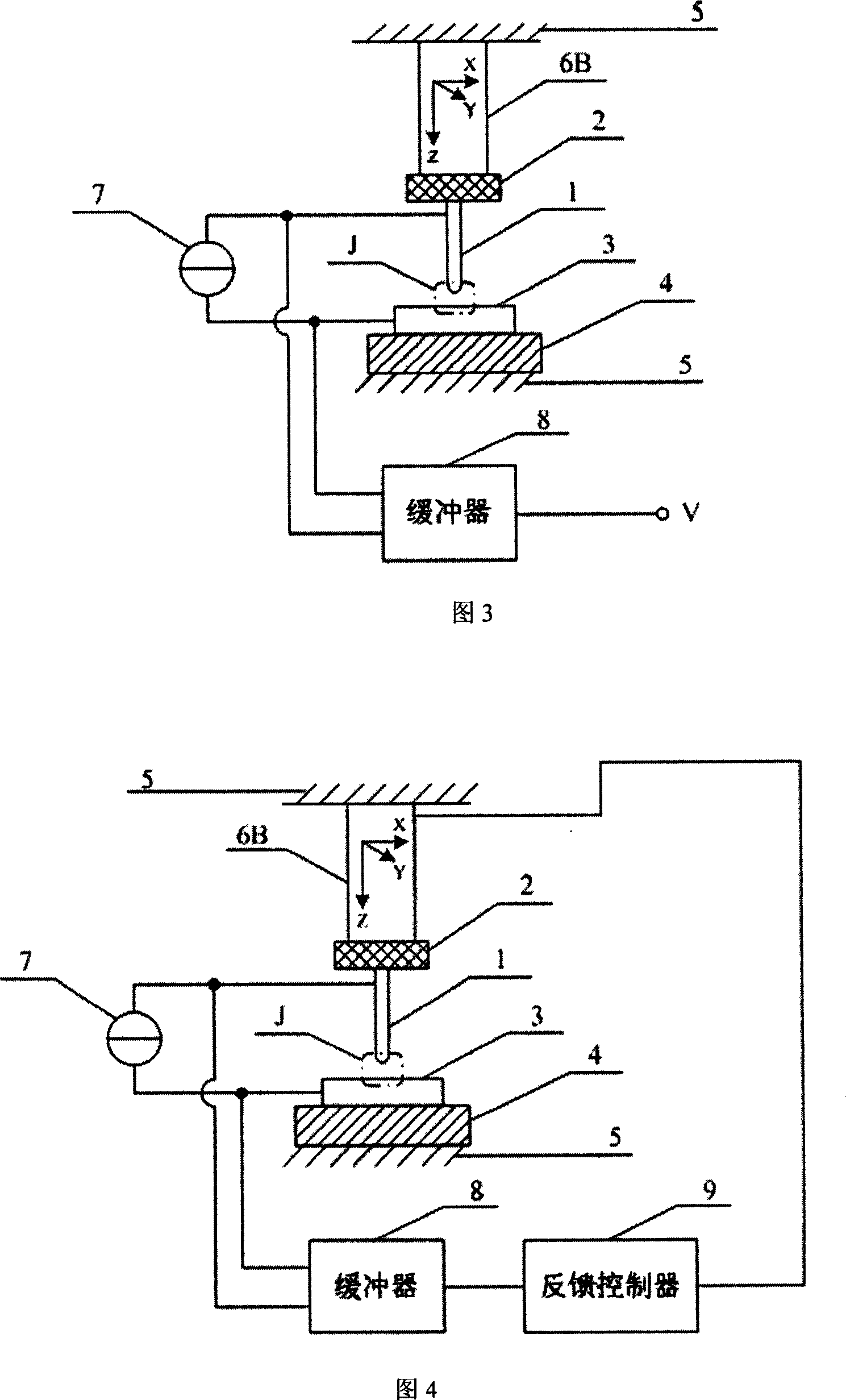
[0032] This embodiment uses the bias current scanning tunneling spectrometer of the present invention for imaging in the contour scanning mode to form an implementation of the bias current scanning tunneling microscope in the contour scanning mode. FIG. 3 is a diagram of this embodiment Structural schematic diagram: replace the Z positioner 6 in embodiment 1 or embodiment 2 with an XYZ positioner 6B. All the other parts are with embodiment 1 or embodiment 2. In this way, the XY positioning of the XYZ positioner 6B can be used to make the probe scan on the sample surface. In the case of keeping the height of the probe constant, the XY scanning signal driving the XY positioner to scan plus the voltage signal output by the buffer 8 is A three-dimensional constant current and voltage image with constant current is given.
[0033] In this embodiment, when the probe 1 scans on the surface ...
PUM
 Abstract
Description
Claims
Application Information