A system to acquire and control data for radiation imaging

A data acquisition and radiation imaging technology, applied in the field of radiation detection, can solve the problems of inconvenient data acquisition and transmission, complex system structure, poor signal anti-interference ability, etc., to improve anti-interference ability, simplify circuits, and reduce electromagnetic interference. Effect

Active Publication Date: 2007-05-16
TSINGHUA UNIV +1
0 Cites 5 Cited by

AI-Extracted Technical Summary

Problems solved by technology

The output of the detector module in the prior art is an analog signal, and the corresponding control system also uses an analog signal...

Method used

Referring to Fig. 2, data and control signal RS485 differential input or output circuit 4 comprise model is the filter capacitance C14-C20 of RS485 chip U5-U11 of MAX3468 and each chip, and the matching resis...

Abstract

The related data acquisition and control system for radiation imaging comprises: an image checkup subsystem, an accelerator, a module circuit for digital detector, the Ethernet, and a module circuit for data acquisition and control. Wherein, the last module circuit includes a differential circuit, a buffer circuit, a generation circuit for data storage and control time sequence, a data storage circuit, a network SCM, an accelerator CP isolation drive circuit, a process circuit for accelerator beam strength information, and a constant voltage power circuit.

Application Domain

Technology Topic

Power circuitsDifferential circuits +13

Image

  • A system to acquire and control data for radiation imaging
  • A system to acquire and control data for radiation imaging
  • A system to acquire and control data for radiation imaging

Examples

  • Experimental program(1)

Example Embodiment

[0036] The following examples are used to illustrate the present invention, but not to limit the scope of the present invention.
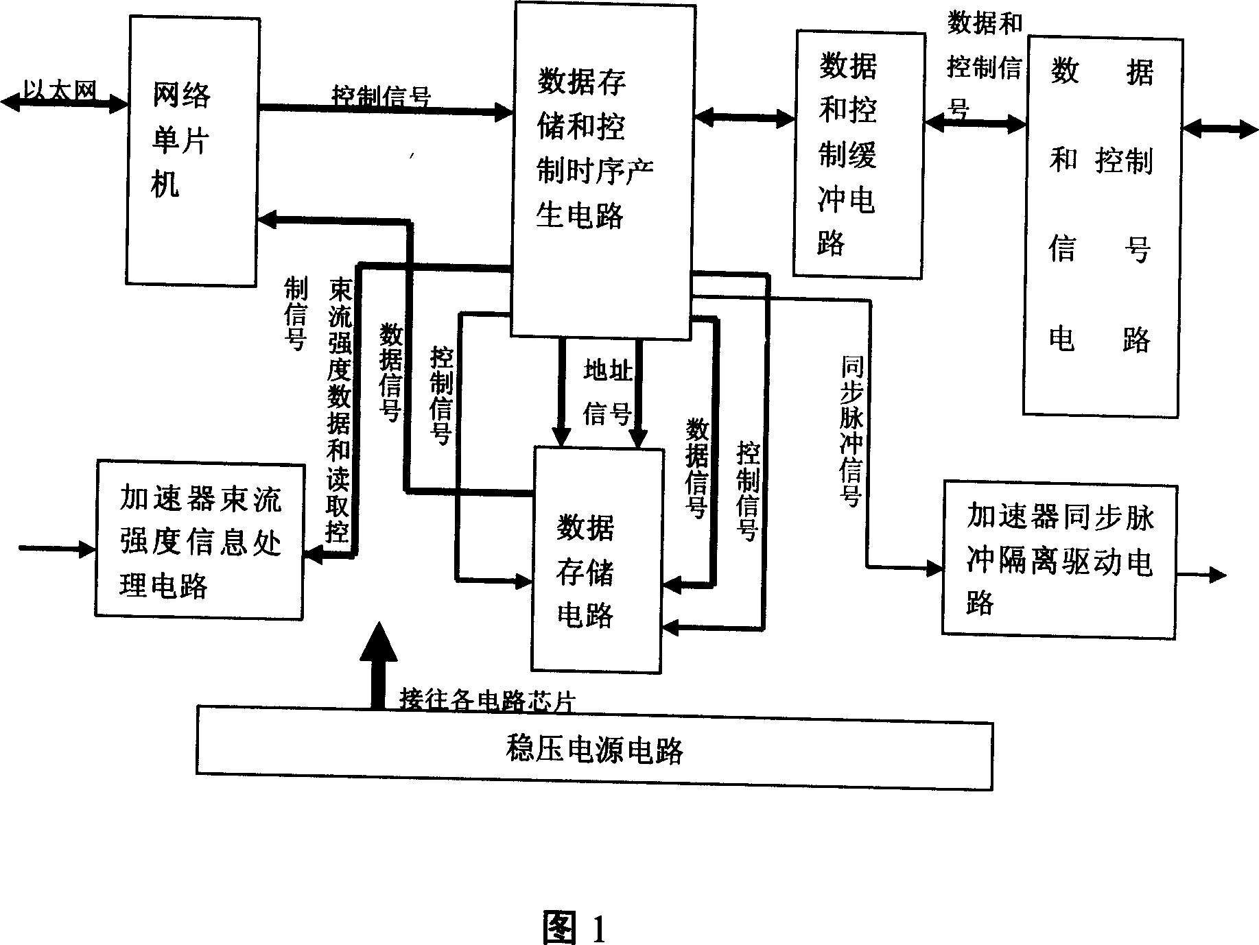
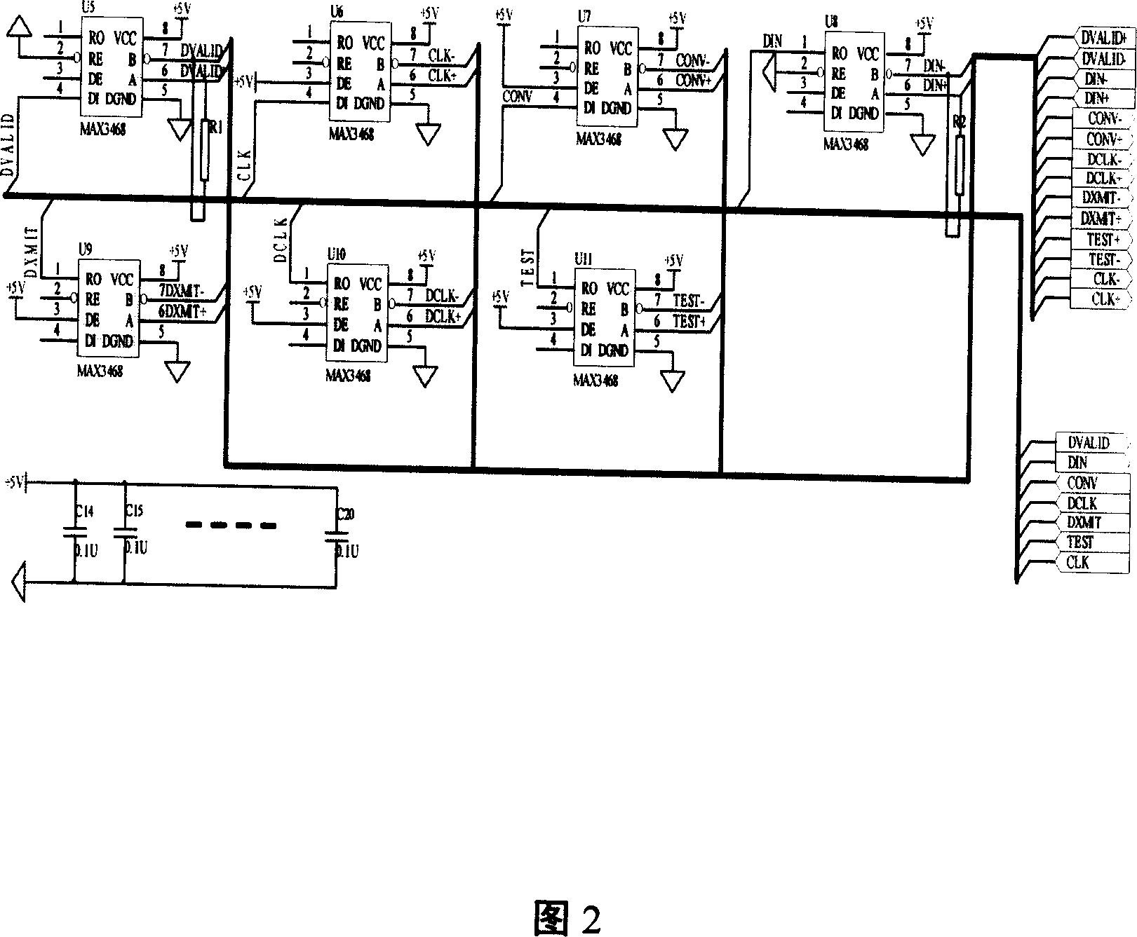
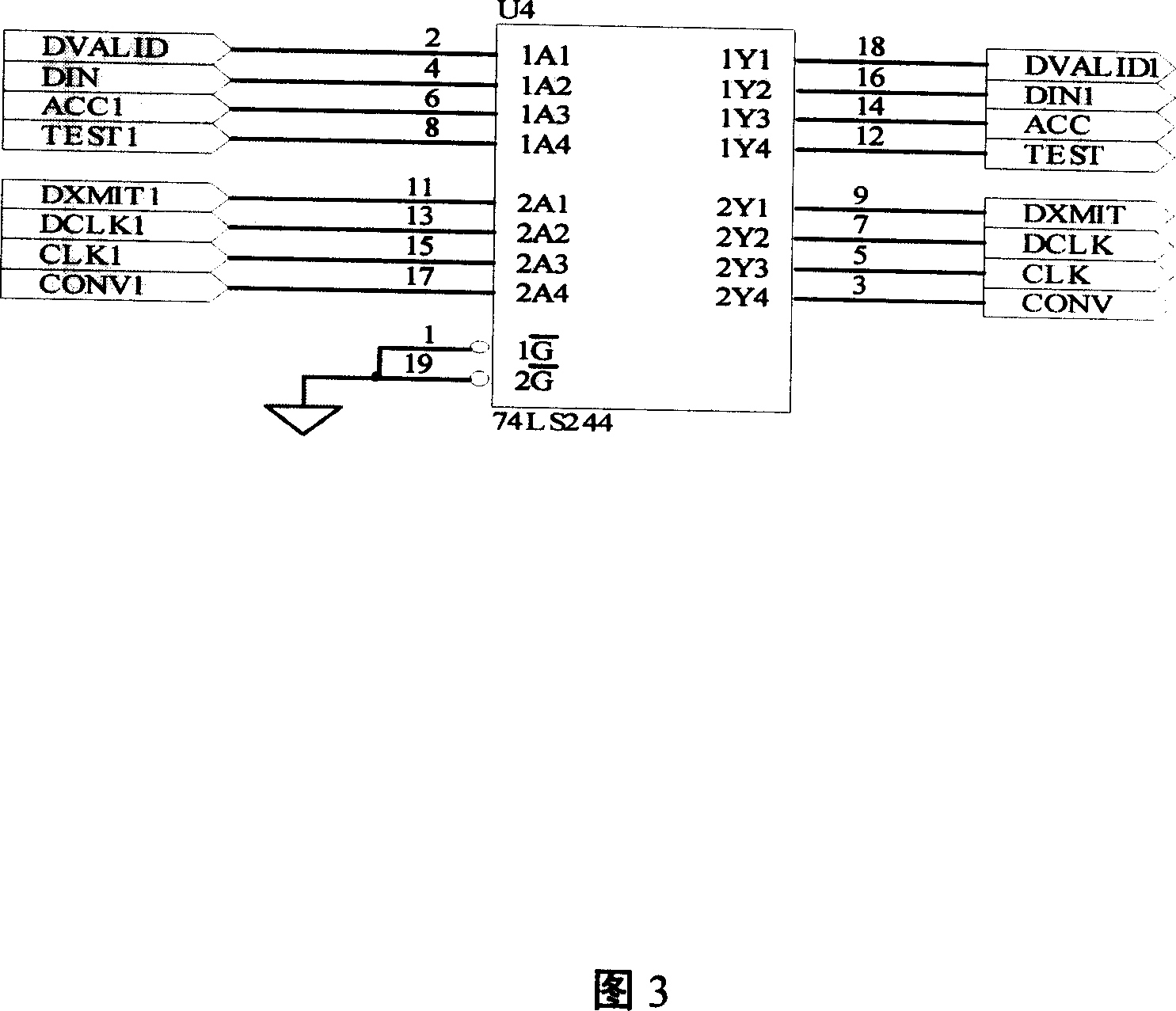
[0037] 1 and 10, the circuit that implements the present invention includes: a differential circuit 4 for receiving detector signals and RS485 data and control signals received or sent, and a buffer circuit 3 for shaping and driving the received or sent data and control signals. , The data and control signal timing generation circuit 2 that receives the command of the network single-chip microcomputer 1 and controls the other circuits, accelerates its beam intensity information processing circuit 5, the accelerator synchronization pulse isolation driving circuit 7, receives the data information and sends it through the Ethernet To the next-level image inspection subsystem 10 and the network single-chip microcomputer 1 that receives the image inspection subsystem commands and sends them to the data and control signal timing generating circuit, a stabilized power supply circuit 8 that provides various power sources.
[0038]The working process is as follows. After the network single-chip microcomputer 1 receives the start instruction of the image inspection subsystem 10, it starts the data storage and control signal timing generating circuit 2 to generate corresponding control signals, and sends out the synchronization required by the accelerator 11 through the buffer circuit 3 and the differential circuit 4. The trigger pulse is sent to the accelerator 11 through the isolation drive circuit 7, and then controls the acquisition of the signal from the detector module circuit 13. The signal of the detector module circuit 13 enters the data storage and control signal timing generation circuit 2 through the differential and buffer circuit. The serially input image data is converted into serial and parallel and stored in the data storage circuit 6. At the same time, the network single-chip microcomputer obtains the previous column of image data that has been stored in another specified address. After storing the data of the detector, it sends it to the network single-chip 1 When an interruption occurs, the network single-chip microcomputer obtains the column of data again, and at the same time sends the last column of image data in the form of Ethernet, alternately reciprocating, and the column by column of image data is sent to the image inspection subsystem 10 for processing and imaging.
[0039] Referring to Figure 10, the data acquisition and control module circuit 9 is connected to the digital detector module circuit 13 through data and control signals and power cables, and is connected to the image inspection subsystem 10 through Ethernet, and through the beam intensity signal double coaxial cable and The synchronized trigger signal cable is connected to the accelerator 11 with a shielded twisted pair cable. The image inspection subsystem 10 can acquire and process image data through the data acquisition and control module circuit 9.
[0040] The implementation of the specific circuit of the present invention will be further described below.
[0041] Refer to Figure 2, the data and control signal RS485 differential input or output circuit 4 includes RS485 chips U5-U11 of the model MAX3468, filter capacitors C14-C20 of each chip, and matching resistors R1 and R2 for anti-reflection, which will require a long distance The transmitted signal is converted into RS485 differential signal, which greatly enhances the anti-interference ability.
[0042] Referring to Figure 3, the data and control signal buffer circuit 3 is composed of an eight-way three-state buffer chip U4 with a model number of 74 (54) LS244. Due to the hysteresis function and strong driving capability of U4, it can reshape and control the data signal and control. Enhance driving ability.
[0043] Referring to Figure 4, the data storage and control sequence generation circuit 2 includes a programmable device U2 of model EP1K30, a chip U19 of EPC2 that provides configuration information for U2, as well as clock oscillator Z1, filter capacitors C21-C37, and pull-up resistor R4. -R7. The data signal lines D0L-D7L, the address signal lines A0L-A13L, and the read-write control line are connected to U3 of the data storage circuit 6 to write data signals into U3. The address signal lines A0R-A13R and the output enable line OER are also connected to U3. CLK1, CONV1, DXMIT1, DVALID1, DCLK1, DIN1, TEST1, ACC1 and other data or control signal lines are connected to U4 of the buffer circuit 3. TMS, TD, DATA0 and other signals are connected to U19, and TCK, TDO, TMS, TDI and other signals can enable FPGA configuration through external lines. REG0-REG7 and INT, RD, RET, DSEL and other control signal lines are connected to the network microcontroller 1. SDO, SCK, CNV are connected with U17 of accelerator beam intensity information processing circuit 5 to obtain beam intensity information. R3 and R13 have an isolation effect and reduce the interference of the clock vibration on other circuits. The frequency of the clock Z1 should be 20MHz or above.
[0044] Referring to FIG. 5, the data storage circuit 6 includes a dual-port RAM chip U3 with a model IDT70V06, and filter capacitors such as C49-C51. A0L-A13L, A0R-A13R, D0R-D7R, OER, R/WL and other address and data lines are connected to U2, and D0L-D7L is connected to the network microcontroller U1. CEL is grounded, OEL, SEML, etc. are connected to the power supply so that the network microcontroller 1 reads the signal through the R/WL signal generated by U2 at any time. SEMR, R/WR, M/S, etc. are connected to the power supply and CER grounding so that U2 can write data at any time through the OER signal.
[0045] Referring to Fig. 6, the network single-chip microcomputer 1 includes a single-chip microcomputer U1 with a model of RCM3200, a C54-C57 filter capacitor, a pull-up resistor R13, and a reset switch S1. The signal lines REG0-REG7, the control lines RD, INT, RET, DSEL, etc. are connected to U2, and the D0R-D7R data lines are connected to U3. The single-chip microcomputer uses REG0-REG7 and RD signals to control U2 (FPGA), and obtains dual-port RAM data through D0R-D7R data lines and DSEL, RD, INT and other control lines. S1 is used to reset the microcontroller, and the microcontroller resets U2 (FPGA) through the RET signal.
[0046] Referring to Fig. 7, the accelerator synchronous pulse isolation driving circuit 7 includes a photoelectric coupling chip U12 with a model of 6N137, a DC-DC low-voltage isolation power supply U21 with a model of B0505S, filter capacitors C52, C53, pull-up resistor R12, and so on. The power supply passes through U21, the synchronization trigger signal ACC is isolated by the optical coupling 12, and the appropriate output current is selected through the pull-up resistor to provide the accelerator and the module with the synchronization trigger pulse signal TRIG-ACC and ground DGND1, which are completely isolated from the module.
[0047] Referring to Fig. 8, the accelerator beam intensity information processing circuit 5 includes an AD8605 operational amplifier U16, an analog-to-digital converter U17 with a model AD7685, a chip U15 with a reference voltage model ADR435, and a filter capacitor C38-C48 and Resistance R9, R10. The VACC bit comes from the accelerator's analog level signal indicating the intensity of the accelerator beam. The SCK, SDO, and CNV signals are connected to U2, and the intensity digital signal after AD conversion is sent to U2.
[0048] Referring to Figure 9, the stabilized power supply circuit 8 includes a stabilized block U14 with a model of 7805, a stabilized block U18 with a model of LM1117-2.5, a stabilized block U20 with a model of LM1117-3.3, and a stabilized block of model LM1117-3.3 U13, resettable fuse F1, filter inductance L1, ferrite L2, capacitors C1-C13 and C58-C61 at all levels, respectively, to provide various power sources +3.3V, C3.3V, +2.5V, + 5V and so on. Use ferrite L2 to connect digital ground and analog ground.

PUM

no PUM

Description & Claims & Application Information

We can also present the details of the Description, Claims and Application information to help users get a comprehensive understanding of the technical details of the patent, such as background art, summary of invention, brief description of drawings, description of embodiments, and other original content. On the other hand, users can also determine the specific scope of protection of the technology through the list of claims; as well as understand the changes in the life cycle of the technology with the presentation of the patent timeline. Login to view more.

Similar technology patents

Delay unit circuit

InactiveCN103647545AImprove anti-interference abilityLogic circuit coupling/interface arrangementsIntermediate stageCapacitance
Owner:WUXI ZGMICRO ELECTRONICS CO LTD

Classification and recommendation of technical efficacy words

  • Improve anti-interference ability
  • Reduce electromagnetic interference

Composite electromagnetic shielding paint based on nano carbon material

InactiveCN105331264AImprove anti-interference abilityGood protection against electromagnetic radiationPolyurea/polyurethane coatingsRadiation-absorbing paintsFerriferrous OxideNickel Carbonyl
Owner:INST OF URBAN ENVIRONMENT CHINESE ACAD OF SCI
Why Eureka
Try Eureka