


Quick Research
Generate reliable direction feasibility study reports for your R&D in just a few steps.

Technical Q&A
Discover and master advanced knowledge NOW. Basics, ideas, possibilities, all at once.

Find Solutions
As an expert in R&D theories, this can generate solutions to your technical problems instantly.

Evaluate Feasibility
Analyze your overall solution with one click, know your potential R&D risks in advance.

Monitor Landscape
Get weekly tech updates, stay abreast of the latest tech innovations and key insights.
Optical waveguide
An optical waveguide and wavelength technology, applied in the direction of optical guide, optical waveguide coupling, measurement device, etc., can solve the problems of reduced detection sensitivity, front-end generation, but also in parts other than the front-end of the probe, increased cost, etc.
- Summary
- Abstract
- Description
- Claims
- Application Information
AI Technical Summary
Problems solved by technology
Method used
Image

Examples
Embodiment Construction
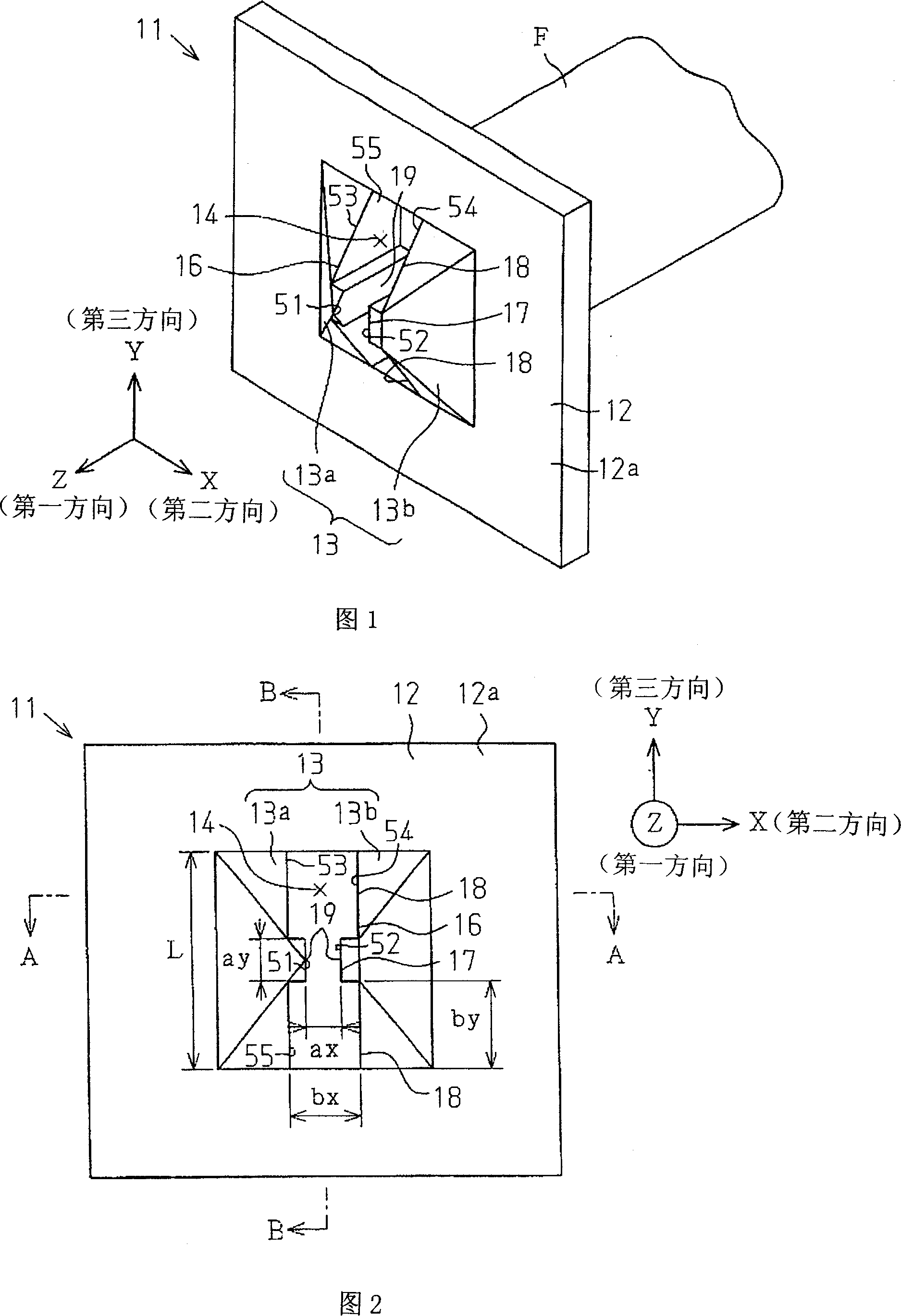
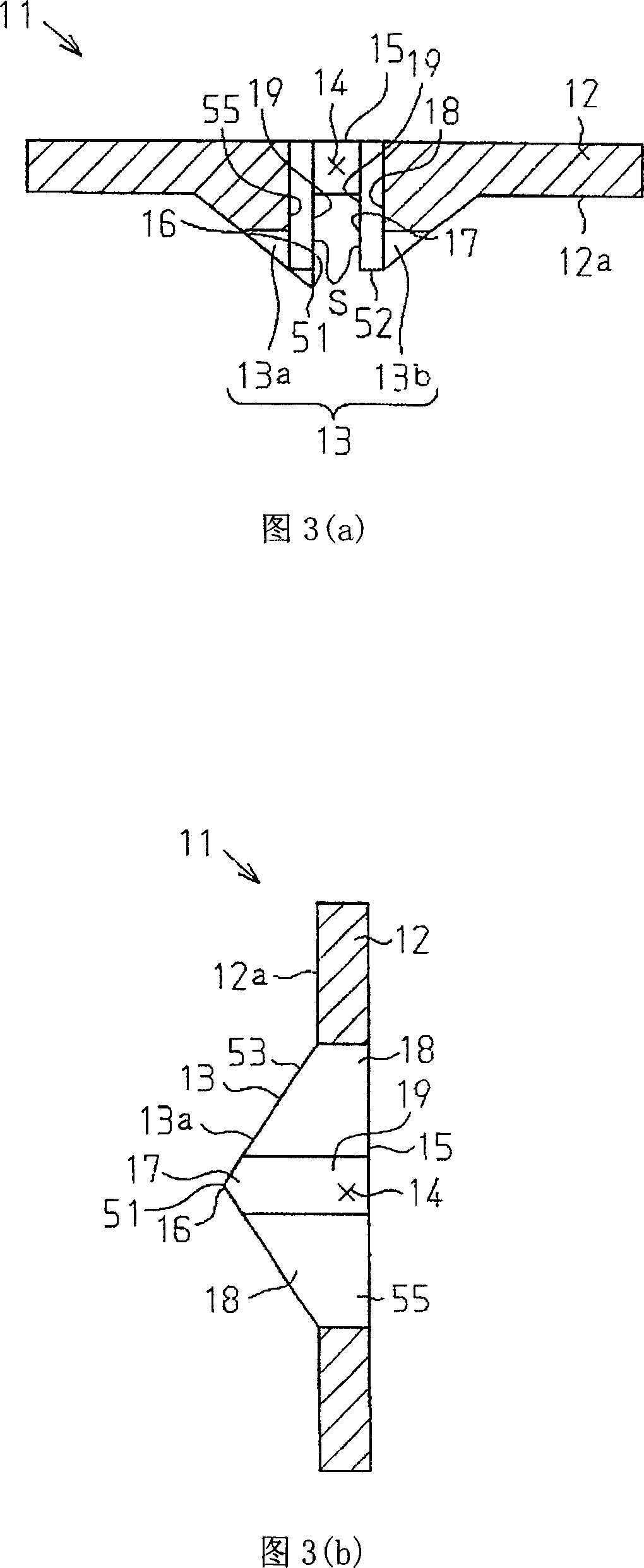
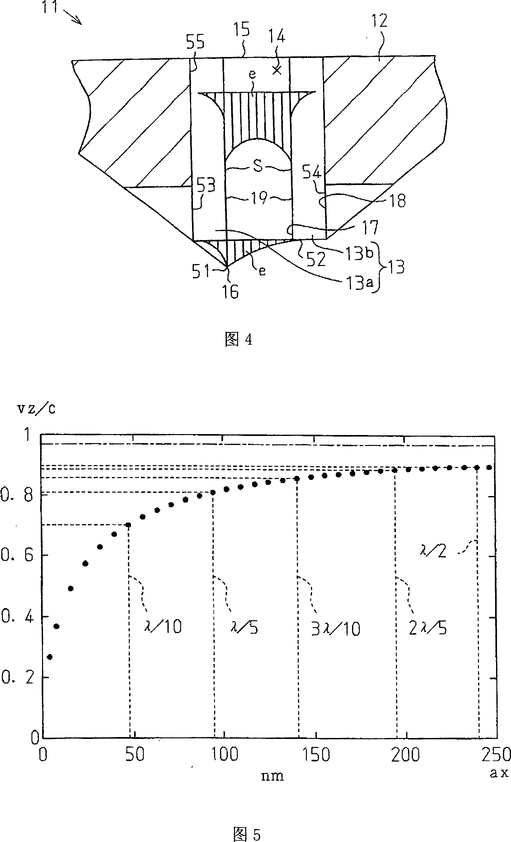
[0025] Hereinafter, the present invention, that is, an optical waveguide device embodied as an optical probe, will be described with reference to FIGS. 1 to 8 with respect to its first embodiment. As shown in FIG. 1 , an optical waveguide device (optical probe) 11 of this embodiment has a metal device body 12 that is rectangular in front view. On the surface portion 12a of the device body 12, a protruding portion 13 that is approximately tapered (approximately square tapered in this embodiment) is formed as a raised portion. The device body 12 and the protrusion 13 are composed of a dielectric having a negative value relative to the real part of the complex permittivity, that is, a negative dielectric (plasmon active medium). In addition, in this embodiment, the case where the wavelength of the light to be transmitted, that is, the fixed wavelength is 488nm (nanometer) is described as an example (hereinafter the same), and as an example, the value of the real part of the relat...
PUM
 Abstract
Description
Claims
Application Information
 - R&D Engineer
- R&D Manager
- IP Professional
- Industry Leading Data Capabilities
- Powerful AI technology
- Patent DNA Extraction
Browse by: Latest US Patents, China's latest patents, Technical Efficacy Thesaurus, Application Domain, Technology Topic, Popular Technical Reports.
© 2024 PatSnap. All rights reserved.Legal|Privacy policy|Modern Slavery Act Transparency Statement|Sitemap|About US| Contact US: help@patsnap.com