

Wafer product and processing method therefor
A processing method and technology for wafers, applied in welding/welding/cutting items, stone processing equipment, laser welding equipment, etc., which can solve problems such as large force and inability to form a reforming zone.
- Summary
- Abstract
- Description
- Claims
- Application Information
AI Technical Summary
Problems solved by technology
Method used
Image

Examples
no. 1 example
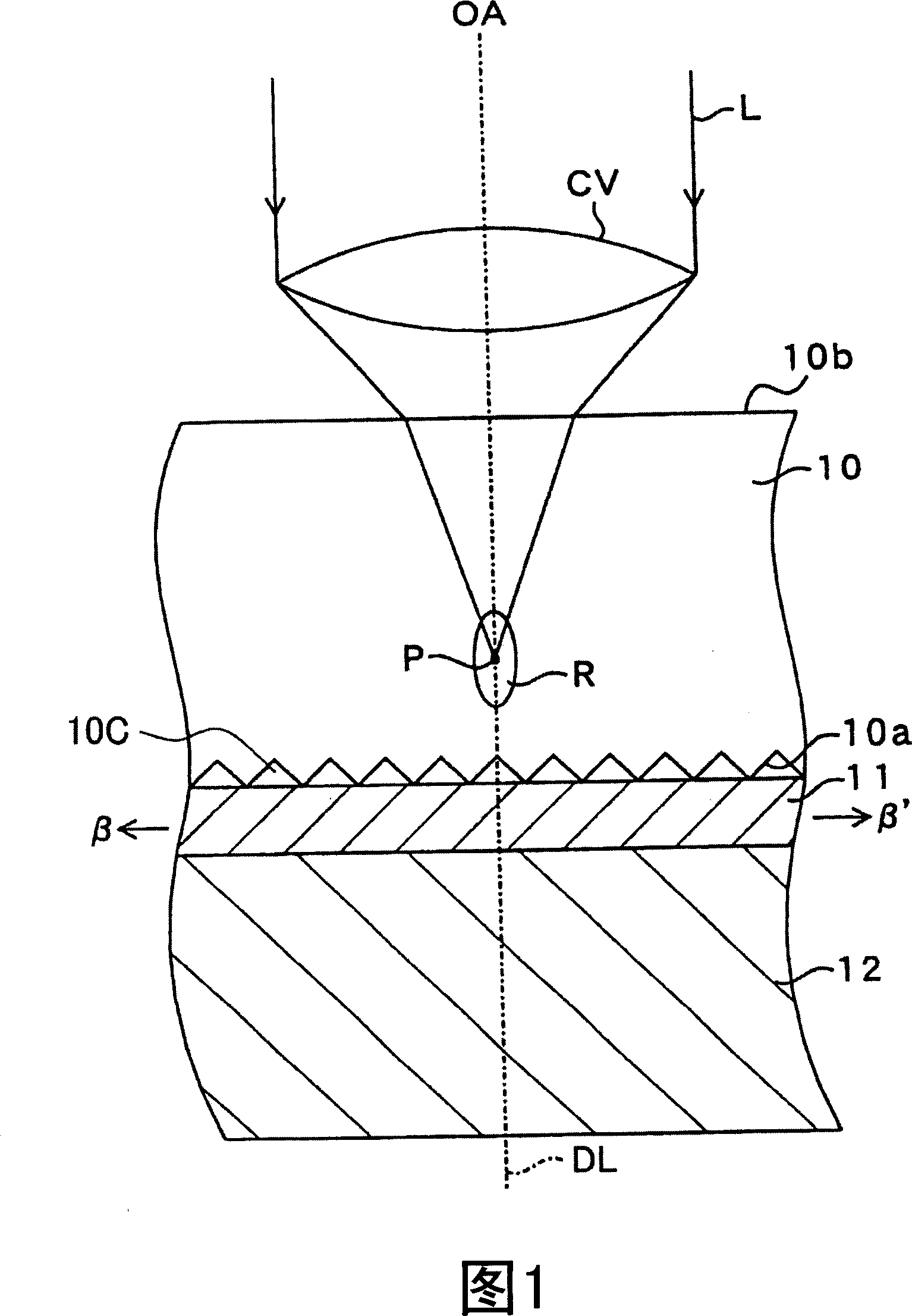
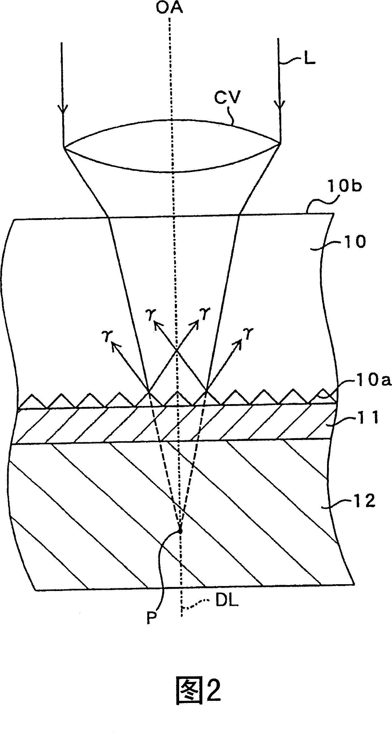
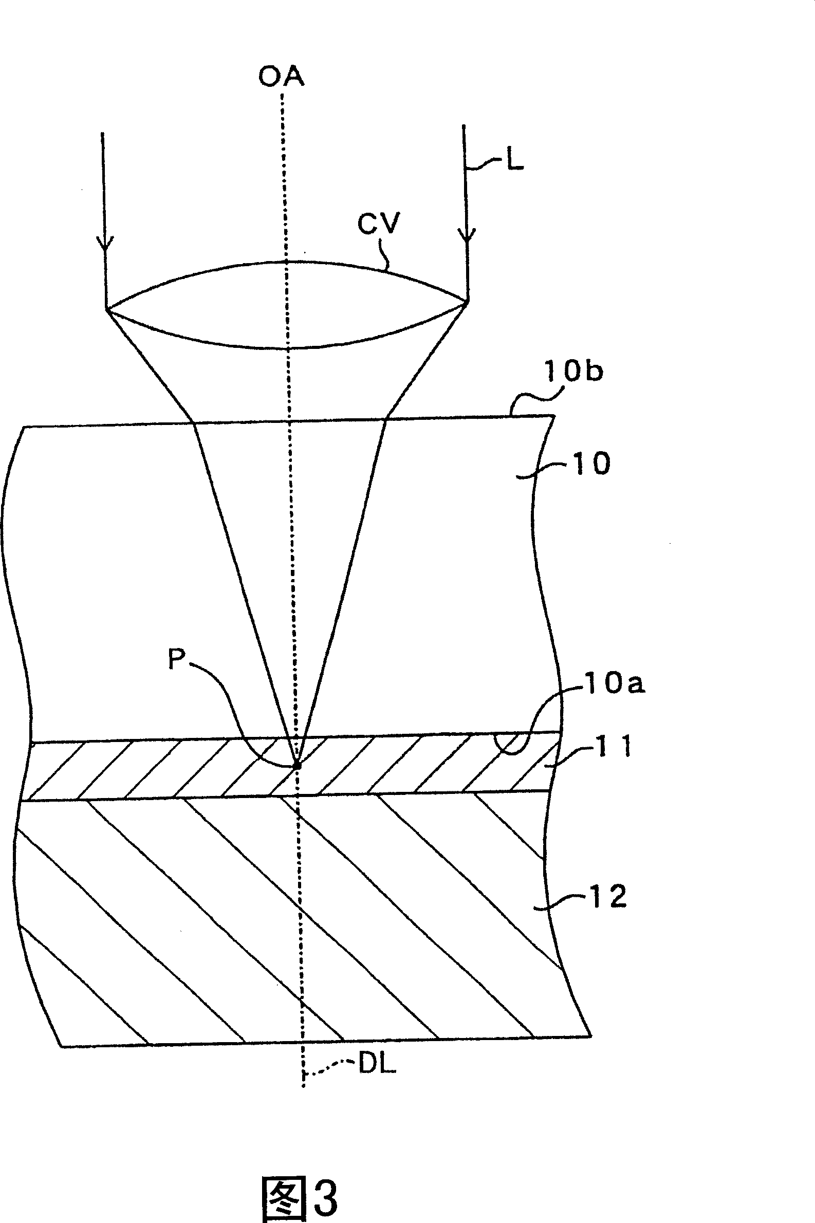
[0044] Referring first to Figures 1 and 2, a bulk silicon wafer 10 is formed from a monocrystalline silicon body of bulk material, the back side 10a of which is a rough surface serving as a protective layer in which substantially uniform protrusions and depressions 10c are formed. . In order to make the rear surface 10a of the wafer 10 a rough surface, ie, a protective layer, any processing method may be used. Examples of treatment methods include: a method of immersing the back surface 10a in an acid solution or an alkaline solution that affects the material used to form the wafer 10 and chemically treats it; and a method of treating the back surface by mechanical polishing such as sandblasting.
[0045] In order to cut and separate the wafer 10 using laser dicing technology, the following procedure is adopted: a cutting sheet (dicing film, dicing tape, expand tape) 11 is attached to the backside 10a of the wafer 10 . The cut sheet 11 is composed of an extensible sheet mater...
no. 2 example
[0079] The second embodiment shown in Figure 8 is different from the first embodiment in the following aspects:
[0080] (2.1) The back surface 10a of the wafer 10 is a smooth surface.
[0081] (2.2) The cutting sheet 11 is composed of a sheet base material 11a and an adhesive material 11b, and the adhesive material 11b is applied to the entire front surface of the sheet base material 11a.
[0082] (2.3) The sheet base material 11a is formed of a stretchable sheet material, and its front face is a smooth surface. The adhesive material 11b is formed of an adhesive sheet having properties of bonding the wafer 10 and the sheet base material 11a together. An example of the adhesive is an acrylic adhesive. The front face of the adhesive material 11b is a rough surface in which substantially uniform protrusions and depressions are formed, so that the adhesive material serves as a protective layer for protecting the base material 11a from laser light L.
[0083] (2.4) The back sur...
no. 3 example
[0089] In the third embodiment shown in FIG. 9, as described in Sections 2.1 and 2.2 with respect to the second embodiment, the front face 10a of the wafer 10 is a smooth surface and the cutting sheet 11 is formed of a sheet base material 11a and an adhesive material 11b. .
[0090] The third embodiment differs from the second embodiment only in the following:
[0091] (3.1) The front face of the sheet base material 11a is a rough surface in which substantially uniform protrusions and depressions are formed. The front of the adhesive material 11b is a smooth surface.
[0092] (3.2) Attach the entire back surface 10a of the wafer 10 to the front surface of the adhesive material 11b. The front face of the sheet base material 11a (in contact with the adhesive material 11b) is a rough surface.
[0093] Therefore, even if the light converging point P is erroneously set to a point beyond the rear surface 10a of the wafer 10, the above-mentioned problem does not arise. Since the ...
PUM
| Property | Measurement | Unit |
|---|---|---|
| wavelength | aaaaa | aaaaa |
Abstract
Description
Claims
Application Information