A MOS FET tube and its manufacturing method

A field effect tube and process technology, applied in the field of semiconductor manufacturing process, can solve the problems of large parasitic capacitance and affecting the speed performance of digital circuits, etc., and achieve the effect of reducing overlapping area, improving speed performance and reducing gate-drain overlapping capacitance

Active Publication Date: 2007-05-30
SHANGHAI HUAHONG GRACE SEMICON MFG CORP
View PDF0 Cites 13 Cited by
  • Summary
  • Abstract
  • Description
  • Claims
  • Application Information

AI Technical Summary

Problems solved by technology

[0003] The parasitic capacitance between the gate drain/source of the MOS field effect transistor manufactured by the method of manufac

Method used


Image

  • A MOS FET tube and its manufacturing method
  • A MOS FET tube and its manufacturing method
  • A MOS FET tube and its manufacturing method

Examples


Embodiment Construction

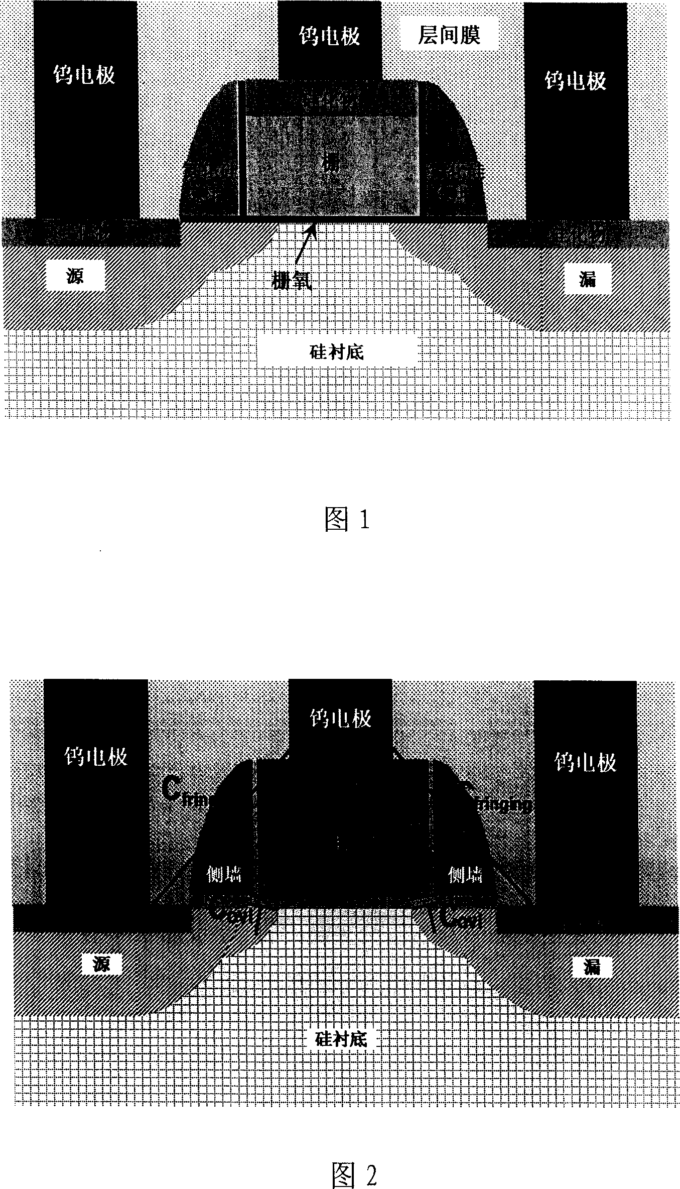
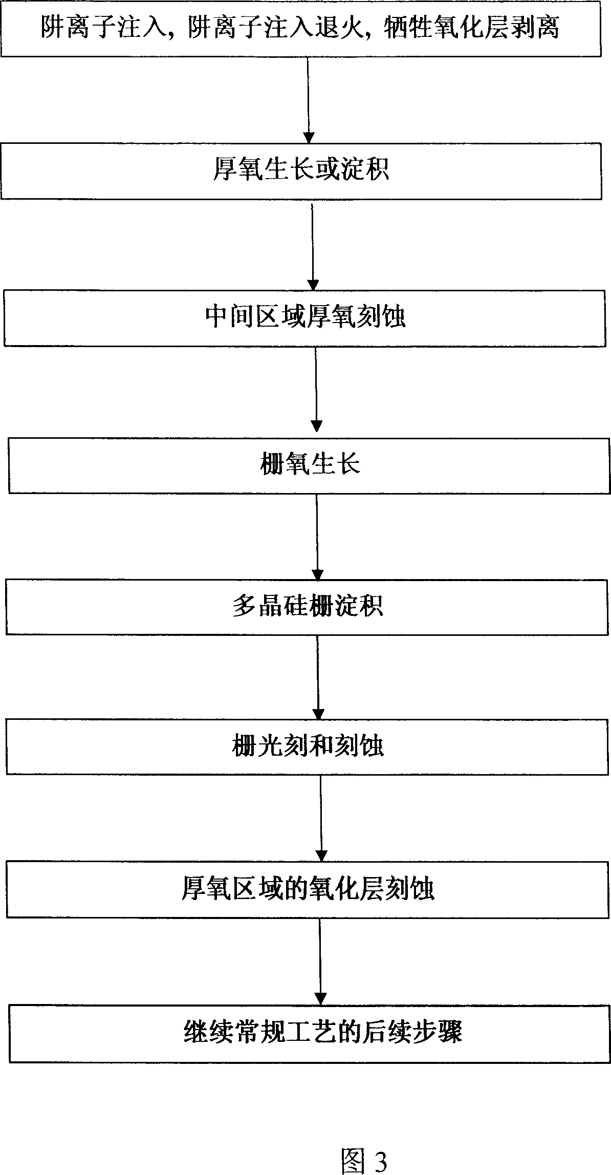
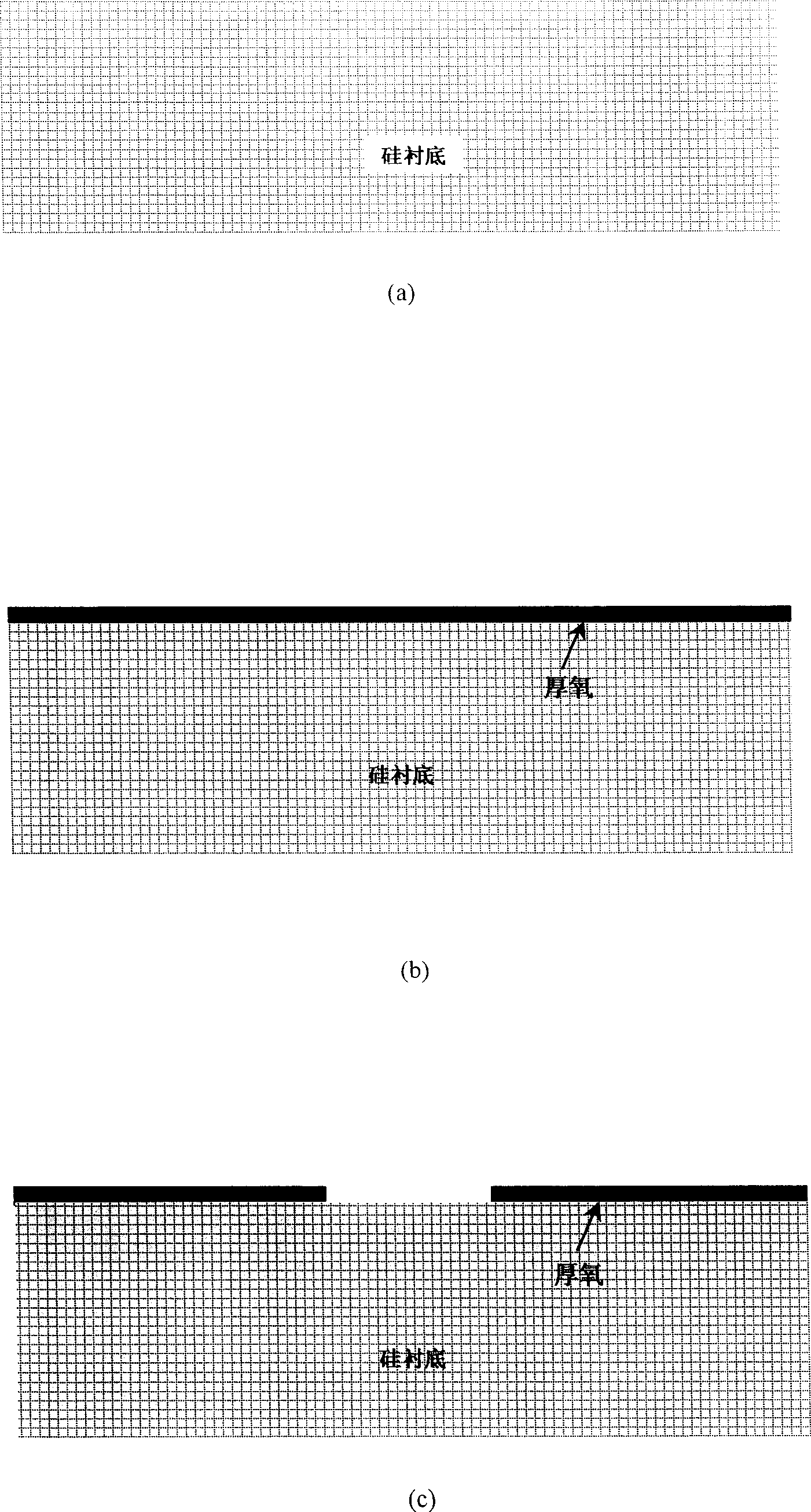
[0016] As shown in Figures 3 and 4, a method for manufacturing a MOS field effect transistor includes the following steps. First, after the trap ion implantation, the trap ion implantation annealing, and the stripping of the sacrificial oxide layer are completed in the conventional process flow, see Fig. 4 (a); Next, thermally grow or deposit a thick oxide layer, the thickness of which should be 2 to 5 times the thickness of the gate oxide grown in subsequent processes, see Figure 4(b). And within the above range, the specific thickness of the thick oxygen needs to be optimized and determined according to the electrical characteristics of the transistor and related process conditions. In the third step, the thick oxygen in the middle area is completely etched away, see Figure 4(c). The edge of the thick oxygen etching region needs to be between the source / drain substrate PN junction and the gate edge to be fabricated in subsequent processes, and the specific position of the ed...


PUM


Abstract

This invention discloses one MOS field effect tube and its process method, which has side wall bottom concaved toward inside. The field effect tube method comprises the following steps: a, injecting well ions for annealing to sacrifice oxidation layer peeling off; b, growing or depositing one layer of thick oxidation layer; c, processing total etching in middle area oxidation; d, growing grating oxidation; e, depositing multiple transistor grating; f, processing light etch on thick oxidation area; g, regular steps after etching.

Description

technical field [0001] The invention relates to a semiconductor manufacturing process, in particular to a MOS field effect transistor and a manufacturing method thereof. Background technique [0002] A cross-sectional structure diagram of an existing MOS field effect transistor is shown in FIG. 1 . In MOS field effect transistors, there will be parasitic capacitance between the gate-drain / source. As shown in FIG. 2, the parasitic capacitance includes gate to drain overlap capacitance (hereinafter referred to as C ovl ) and gate todrain fringing capacitance (hereinafter referred to as C fringing ). In the conventional semiconductor manufacturing process flow of the prior art, the sidewall of the gate is generally vertical and flat, and the parasitic capacitance of the MOS field effect transistor with the existing structure is usually relatively large. Parasitic capacitance usually affects the speed performance of digital circuits. The larger the capacitance, the worse th...

Claims


Application Information

Patent Timeline
IPC IPC(8): H01L29/423H01L29/78H01L21/336
Inventor 伍宏
Owner SHANGHAI HUAHONG GRACE SEMICON MFG CORP
Why Eureka
Try Eureka