A MOS FET tube and its manufacturing method

A technology of field effect transistors and substrates, applied in semiconductor/solid-state device manufacturing, electrical components, circuits, etc., can solve problems affecting the speed performance of digital circuits and reduce the intrinsic performance of transistors, so as to improve speed performance and reduce gate leakage Overlap capacitance, effect of reducing gate-drain fringe capacitance

Inactive Publication Date: 2007-05-30
SHANGHAI HUA HONG NEC ELECTRONICS
View PDF0 Cites 8 Cited by
  • Summary
  • Abstract
  • Description
  • Claims
  • Application Information

AI Technical Summary

Problems solved by technology

But the above approach is at the expense of reducing the intrinsic performance of the transistor
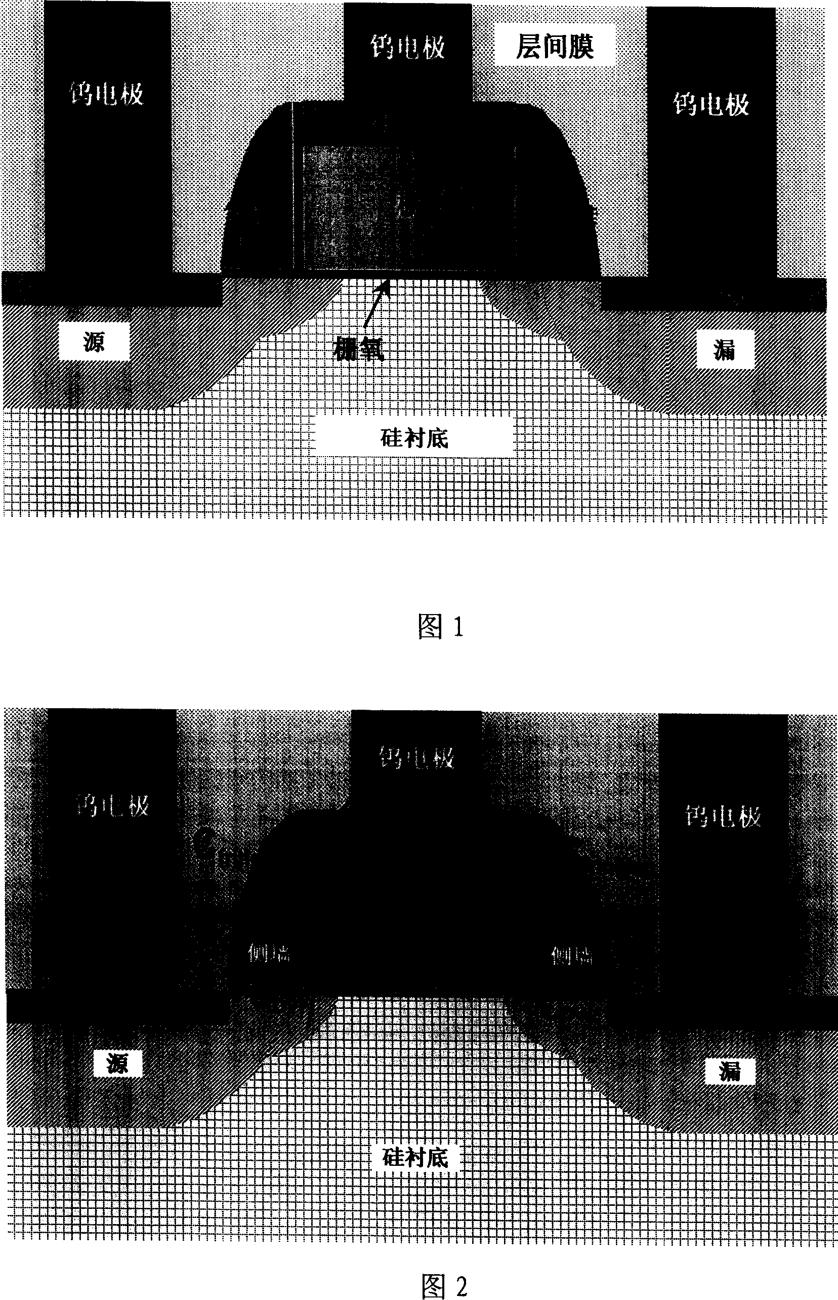
[0003] The parasitic capacitance between the gate-drain / source of the MOS field-effect transistor produced by the method of the prior art, such as the gate-drain overlapping capacitance and the gate-drain edge capacitance is relatively large, which will affect the speed performance of the digital circuit

Method used


Image

  • A MOS FET tube and its manufacturing method
  • A MOS FET tube and its manufacturing method
  • A MOS FET tube and its manufacturing method

Examples


Embodiment Construction

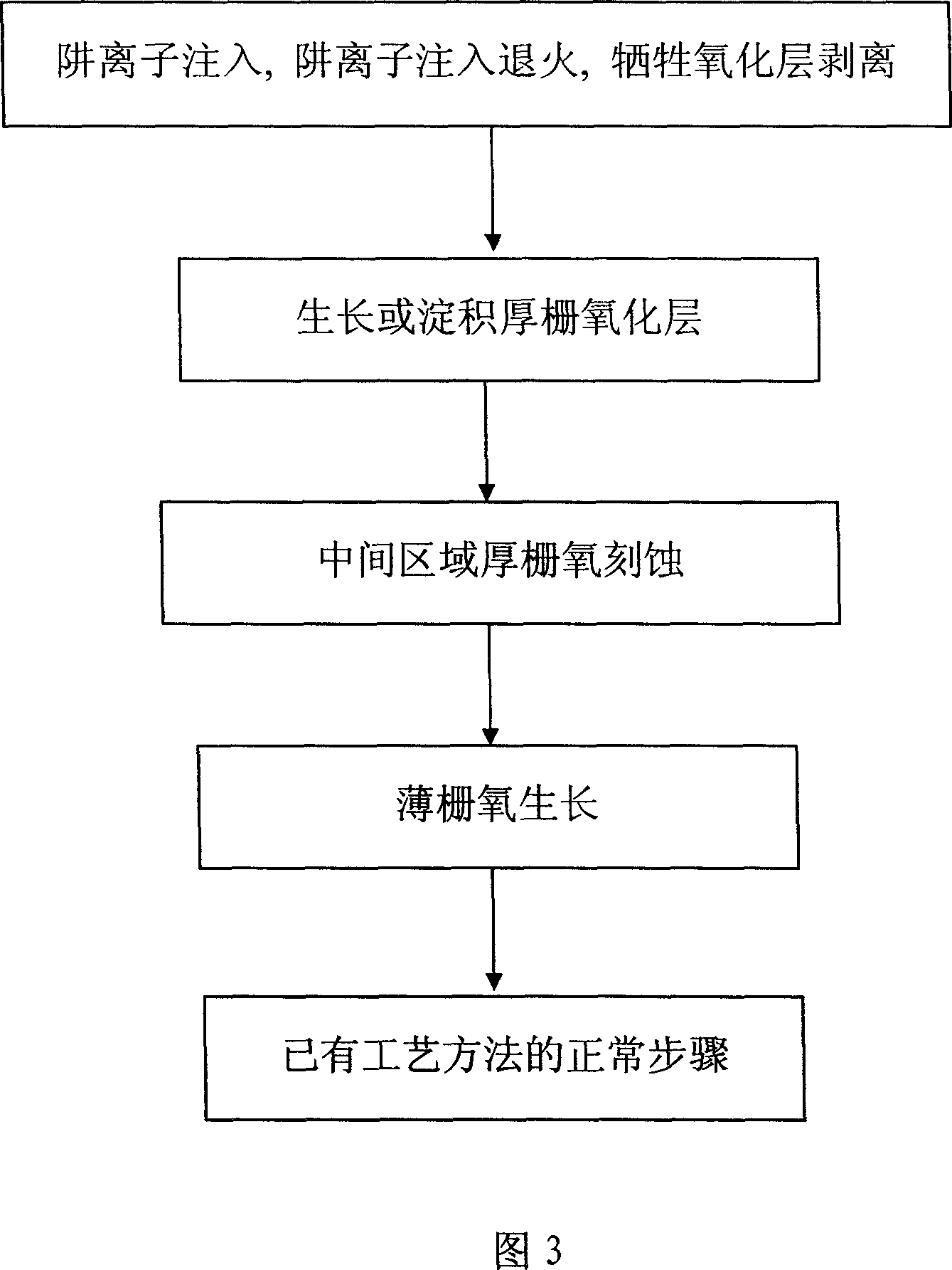
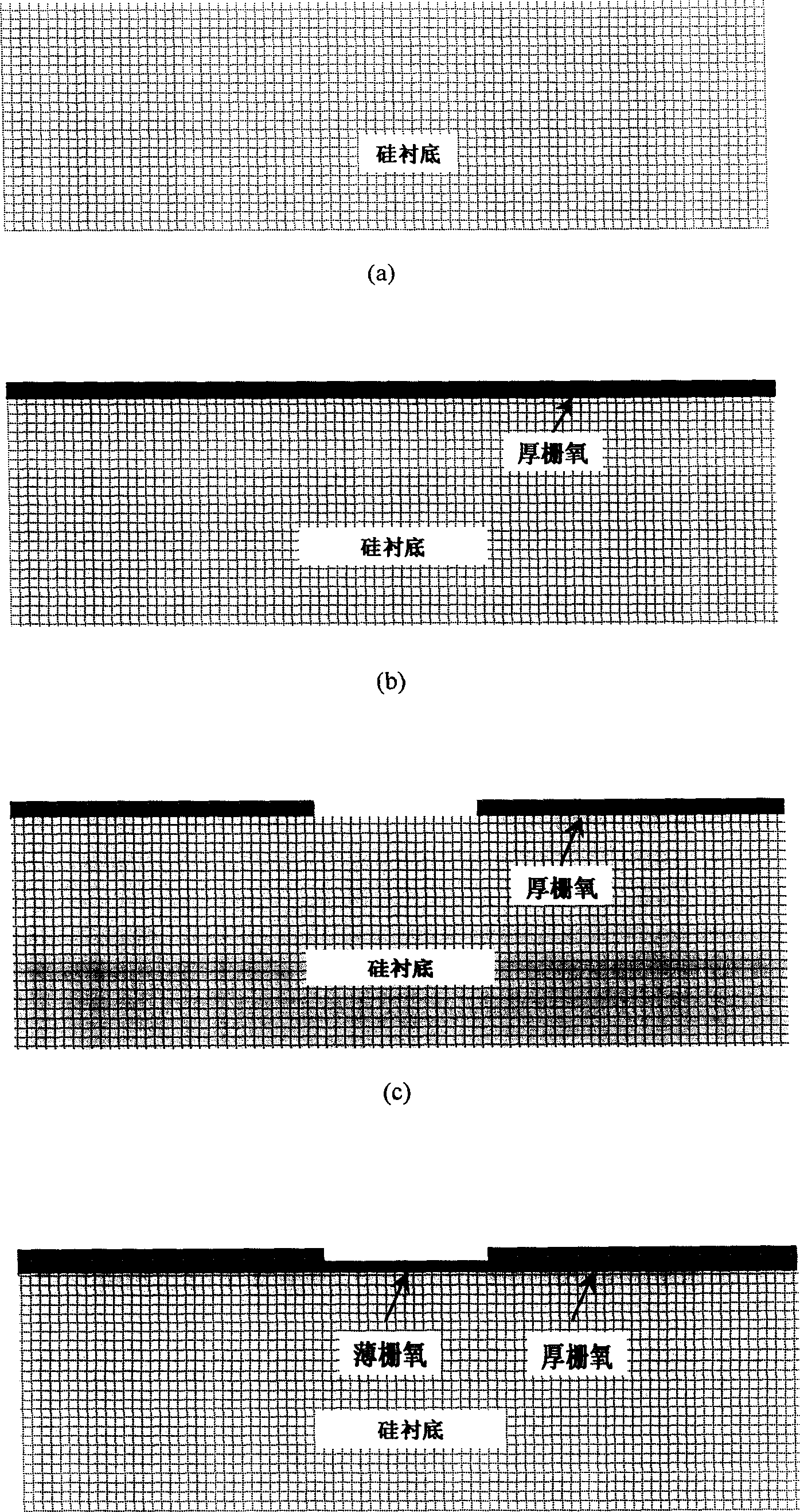
[0016] As shown in Figures 3 and 4, a method for manufacturing a MOS field effect transistor includes the following steps. First, the well ion implantation, the well ion implantation annealing, and the stripping of the sacrificial oxide layer are completed in the conventional process flow, as shown in Figure 4 ( a); The second step is to thermally grow or deposit a thick gate oxide layer. The thickness of the thick gate oxide should be 2 to 5 times the thickness of the thin gate oxide grown in the subsequent process, see FIG. 4(b). Within the above range, the specific thickness of the thick gate oxide is optimally selected and determined according to the electrical characteristics of the transistor and related process conditions. The third step is to completely etch away the thick gate oxide in the middle region, see Figure 4(c). The edge of the thick gate oxide etching region is between the source / drain-substrate PN junction and the edge of the gate in the subsequent process....


PUM


Abstract

This invention discloses one MOS field effect tube and its process method, which has the following steps: a, injecting well ion and annealing and sacrifice oxidation layer for peeling off; b, growing or depositing one layer of grating oxidation layer; c, totally etching middle area grating oxidation; d, growing film grating oxidation; e, the current process method steps are applicable for this invention.

Description

technical field [0001] The invention relates to a semiconductor manufacturing process, in particular to a MOS field effect transistor and a manufacturing method thereof. Background technique [0002] A cross-sectional structure diagram of an existing MOS field effect transistor is shown in FIG. 1 . In MOS field effect transistors, there will be parasitic capacitance between the gate-drain / source. As shown in FIG. 2, the parasitic capacitance includes gate to drain overlap capacitance (hereinafter referred to as C ovl ) and gate todrain fringing capacitance (hereinafter referred to as C fringing ). In the conventional semiconductor manufacturing process flow of the prior art, the thickness of the gate oxide under the gate is generally uniform, and the parasitic capacitance of the MOS field effect transistor with the existing structure is usually relatively large. Parasitic capacitance usually affects the speed performance of digital circuits. The larger the capacitance, ...

Claims


Application Information

Patent Timeline
Patent Type & Authority Applications(China)
IPC IPC(8): H01L29/78H01L29/423H01L21/336H01L21/283
Inventor 伍宏
Owner SHANGHAI HUA HONG NEC ELECTRONICS
Why Eureka
Try Eureka