Method for preparing carbon nano tube array

A technology of carbon nanotube array and deposition method, which is applied in the direction of oriented carbon nanotubes, nanotechnology, nanotechnology, etc., can solve problems such as difficult application, increased manufacturing cost, and inability to guarantee the straightness of carbon nanotube arrays. Clean smooth, high surface density results

Active Publication Date: 2007-06-13
BEIJING FUNATE INNOVATION TECH +1
View PDF0 Cites 16 Cited by
  • Summary
  • Abstract
  • Description
  • Claims
  • Application Information

AI Technical Summary

Problems solved by technology

The formation of carbon nanotubes by arc discharge and pulsed laser evaporation has the following disadvantages: (1) the yield of carbon nanotubes is low; (2) carbon nanotubes are mixed with other carbon nanoparticles, thus resulting in the purity of carbon nanotubes Very low, also need complex purification process, increase manufacturing cost; (3) the growth direction of carbon nanotubes cannot be controlled, and the formed carbon nanotubes are disordered and chaotic, which is difficult to be applied in industry
However, because during the growth of carbon nanotubes, amorphous carbon will be deposited on the outer surface of carbon nanotubes at the same time, so that the van der Waals force between carbon nanotubes is reduced.
Therefore, the van der Waals force between the carbon nanotubes in the carbon nanotube array grown by this method is weak, so the straightness of the carbon nanotube array cannot be guaranteed.

Method used


Image

  • Method for preparing carbon nano tube array
  • Method for preparing carbon nano tube array

Examples


preparation example Construction

[0013] A method for preparing a carbon nanotube array provided by an embodiment of the present invention comprises the following steps:

[0014] (1) Provide a smooth base. The smooth substrate can be polished silicon wafer, polished silicon dioxide wafer and polished quartz wafer, and its surface flatness is preferably less than 300 nanometers; it can make the subsequent carbon nanotube growth catalyst layer can be evenly attached to the substrate surface.

[0015] (2) Forming a catalyst layer on the surface of the smooth substrate. The catalyst layer can be deposited on the substrate by electron beam evaporation or magnetron sputtering, and its thickness is generally 3-6 nanometers. The material of the catalyst layer can be selected from one or a combination of iron, cobalt, nickel or their alloys. The deposition rate for forming the catalyst layer, that is, the thickness change rate, is preferably lower than 0.5 nm / s, which enables the catalyst to be uniformly attached to...

no. 1 example

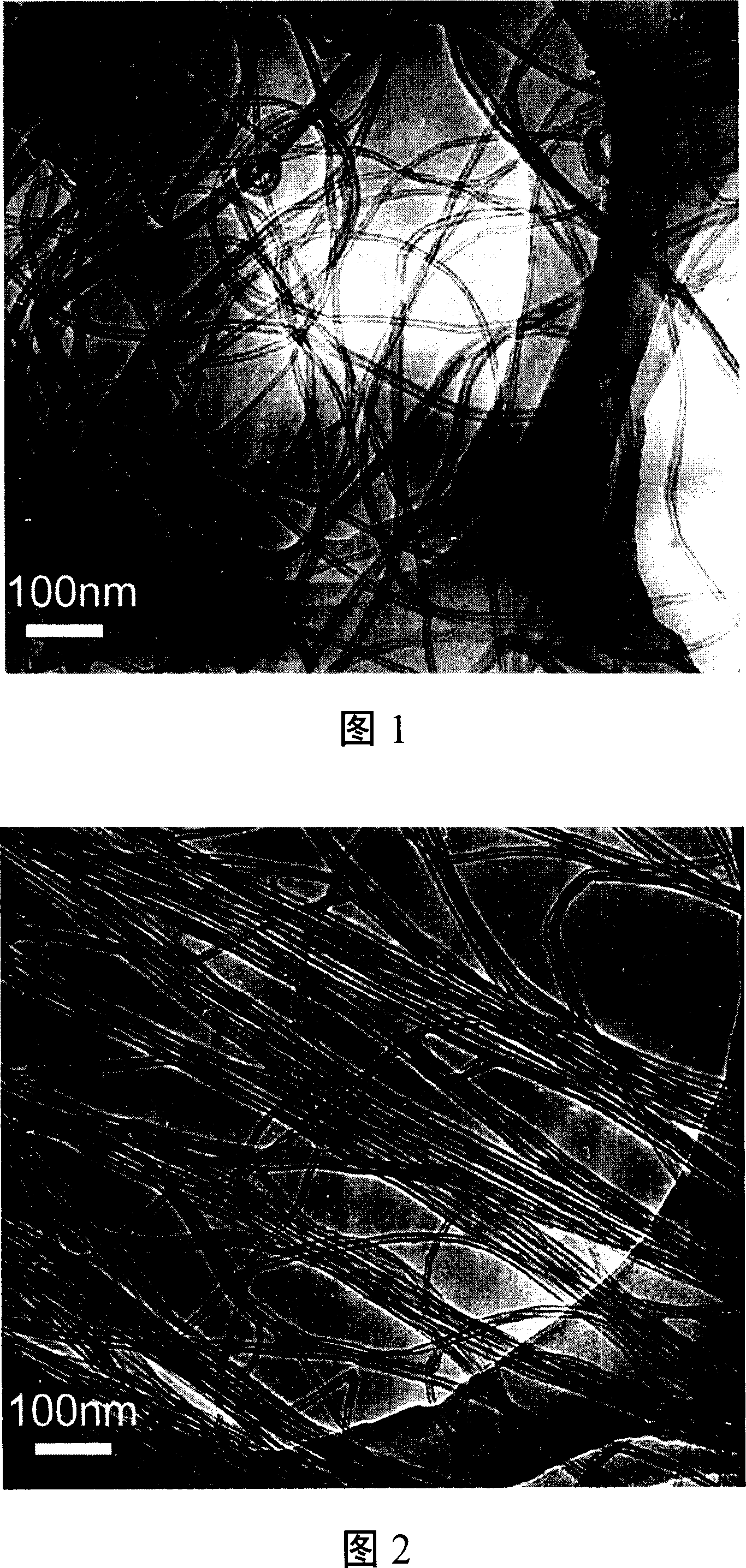
[0019] In this embodiment, carbon nanotube arrays are prepared by atmospheric pressure chemical vapor deposition. Usually, the pressure range of the atmospheric pressure chemical vapor deposition method is 10-760 Torr. In this embodiment, a polished silicon wafer is selected as the substrate, iron is selected as the catalyst, and a mixed gas of acetylene and hydrogen is selected as the reaction gas. An iron catalyst layer with a thickness of 3 to 6 nanometers is formed on a polished silicon substrate by using an electron beam evaporation method at a deposition rate of 0.01 nanometers / second. The substrate formed with the iron catalyst layer is put into a quartz furnace, fed with hydrogen and heated to 620-700 degrees Celsius. Add acetylene into the quartz furnace and keep it for 10-30 minutes; then a carbon nanotube array can be obtained. Wherein, the flow rate of acetylene can be 30 sccm; the flow rate of hydrogen gas can be set to 300 sccm; during the growth process of the...


PUM

PropertyMeasurementUnit
thicknessaaaaaaaaaa
pore sizeaaaaaaaaaa

Abstract

This invention provides a preparation method for carbon nanometer-tubes including: providing a smooth base, forming a catalyst layer on the surface of the base with the rate lower than 0.5nm / s of thickness change, penetrating a reaction gas to apply a chemical gas-deposition method under a preset temperature to let a carbon nano-tube come out from the array.

Description

【Technical field】 [0001] The invention relates to a method for preparing a carbon nanotube array, in particular to a method for preparing a super-parallel carbon nanotube array. 【Background technique】 [0002] Due to the unique electrical properties of carbon nanotubes, their applications in the fields of nano-integrated circuits and single-molecule devices have immeasurable prospects. At present, people have been able to manufacture devices such as field effect transistors and NOR gates based on carbon nanotubes in small quantities in the laboratory. With the application of carbon nanotubes, great progress has been made in the synthesis of large-area carbon nanotube arrays, which are expected to be applied to devices such as field emission flat panel displays. [0003] At present, there are three main methods for preparing carbon nanotubes: arc discharge method, pulsed laser evaporation method and chemical vapor deposition method. The formation of carbon nanotubes by arc ...

Claims


Application Information

Patent Timeline
Patent Type & Authority Applications(China)
IPC IPC(8): C01B31/02
CPCC01B2202/08B82Y40/00C01B31/0233B82Y30/00C01B32/162
Inventor 张晓波姜开利范守善
Owner BEIJING FUNATE INNOVATION TECH
Why Eureka
Try Eureka