Semiconductor structure and manufacture method thereof

一种制造方法、半导体的技术,应用在半导体/固态器件制造、半导体器件、半导体/固态器件零部件等方向,能够解决半导体结构脆弱等问题,达到消除负面影响、降低可能性、降低寄生电容值的效果

Inactive Publication Date: 2007-06-13
TAIWAN SEMICON MFG CO LTD
View PDF0 Cites 2 Cited by
  • Summary
  • Abstract
  • Description
  • Claims
  • Application Information

AI Technical Summary

Problems solved by technology

Formed semiconductor structure is fragile due to lack of etch stop layer

Method used


Image

  • Semiconductor structure and manufacture method thereof
  • Semiconductor structure and manufacture method thereof
  • Semiconductor structure and manufacture method thereof

Examples


Embodiment Construction

[0046] Embodiments of the present invention will be described with reference to the cross-sectional views of FIGS. 1-9B .

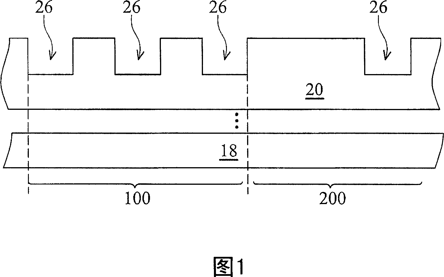
[0047] First, please refer to FIG. 1 , which shows a situation where a low-k dielectric layer 20 is formed on a substrate 18 . The substrate 18 (or, the low-k dielectric layer 20 ) includes a region 100 and a region 200 . The low-k dielectric layer 20 is preferably an inter-metal dielectric (IMD) with a dielectric constant lower than 2.5 (hereinafter referred to as a very low-k dielectric layer). . The low-k dielectric layer 20 preferably includes nitrogen, carbon, hydrogen, oxygen, fluorine, and combinations thereof. Here, a plurality of openings 26 are formed in the low-k dielectric layer 20 by etching.

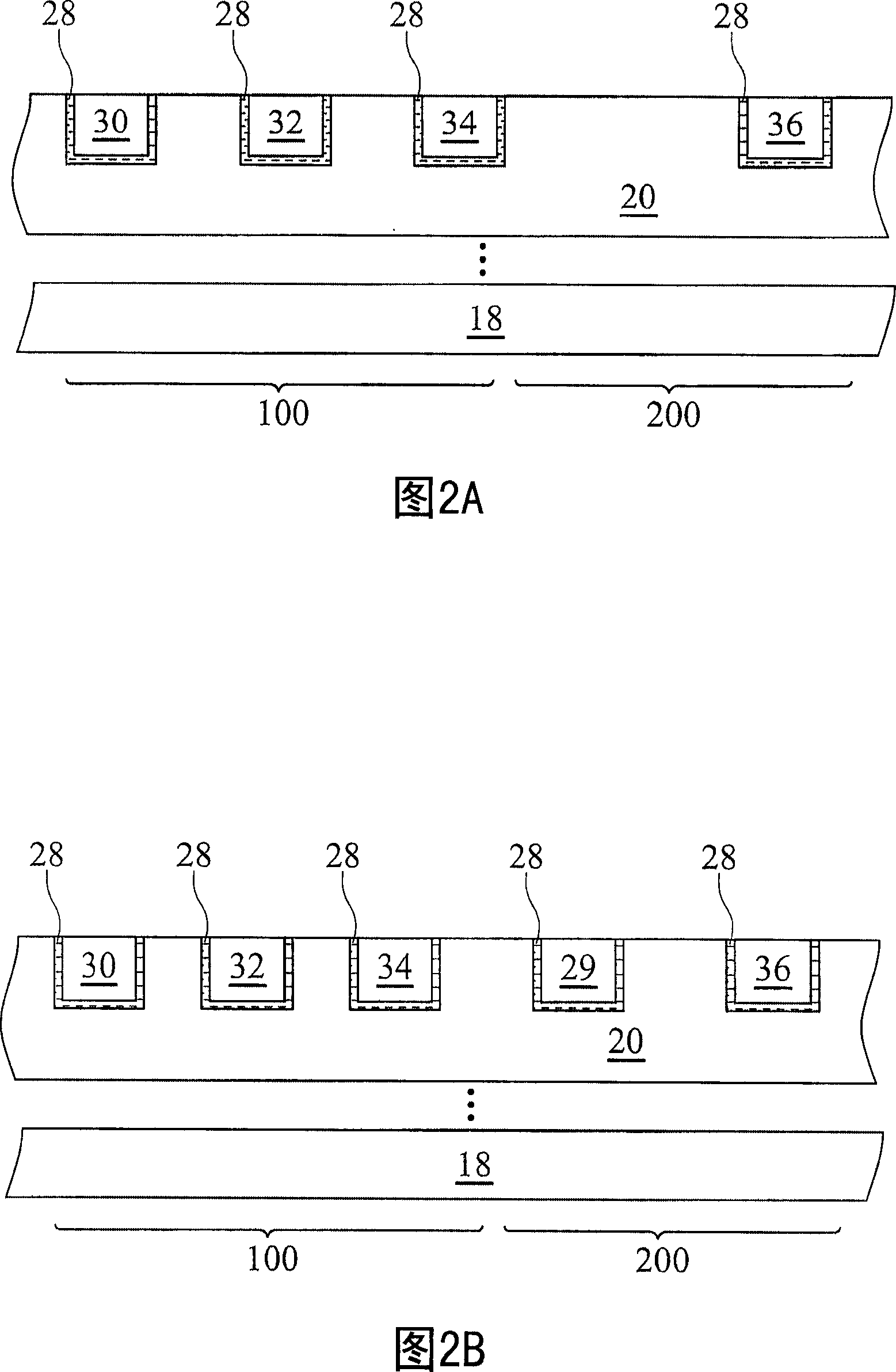
[0048] Please refer to FIG. 2A , which shows a situation where a diffusion barrier layer 28 and wires (conductive members) 30 , 32 , 34 , 36 are then formed in the opening 26 . The diffusion barrier layer 28 is formed on the bottom and sidewalls of...


PUM

PropertyMeasurementUnit
compressive strengthaaaaaaaaaa

Abstract

A semiconductor structure and a fabricating method of the same are provided. The semiconductor structure includes a substate; a first low dielectric constant dielectric layer covering the substate and having a first area and a second area; a plurality of conductive member in the low dielectric constant dielectric layer; an upper lid layer positioned on at least a part of the conductive member; and a dielectric upper lid layer covering the second area of the first low dielectric constant dielectric layer and not covering the first area, wherein the conductive member positioned in the second area has a wider space than the conductive member positioned in the first area. The dielectric upper lid layer preferably has an invariable compressing stress.

Description

technical field [0001] The invention relates to an interconnection structure of an integrated circuit, and in particular to a damascene process. Background technique [0002] In general, an integrated circuit includes a plurality of metal line patterns separated by spacers of interconnect lines, and interconnect lines such as bus lines, bit lines, word lines, and logic interconnect lines. (logic interconnect lines) multiple inline circuit. These vertically separated patterns of metal lines are electrically connected by vias formed therebetween. Metal lines are formed within trench-like openings and generally extend generally parallel to the semiconductor substrate. According to different circuit technologies, the above-mentioned semiconductor device may include eight or more layers of metal circuits, so as to meet the requirements of device appearance and miniaturization. [0003] One of the existing methods of forming metal lines or vias is the so-called damascene. In g...

Claims


Application Information

Patent Timeline
Patent Type & Authority Applications(China)
IPC IPC(8): H01L23/522H01L21/768
CPCH01L23/53295H01L2924/0002H01L21/76849H01L21/76829H01L23/528H01L21/76807H01L2924/00
Inventor 吴仓聚章勋明
Owner TAIWAN SEMICON MFG CO LTD
Why Eureka
Try Eureka