Image sensor devices and photoelectric element

An image sensor and image sensing technology, applied in electrical components, image communication, electric solid-state devices, etc., can solve the problem of photodiode leakage, low signal-to-noise ratio, affecting the electrical properties of image sensing devices and sensing results, etc. problem, to achieve the effect of reducing dark current, high signal-to-noise ratio, and increasing computing speed

Active Publication Date: 2007-06-20
TAIWAN SEMICON MFG CO LTD
View PDF2 Cites 7 Cited by
  • Summary
  • Abstract
  • Description
  • Claims
  • Application Information

AI Technical Summary

Problems solved by technology

However, the metal silicide located on the gate structure is a metastable substance, and the contained metal components will still diffuse to the photodiode area in the subsequent process, causing leakage spots of the photodiode. And obtain a low signal-to-noise ratio, thereby affecting the electrical properties and sensing results of the image sensing device

Method used


Image

  • Image sensor devices and photoelectric element
  • Image sensor devices and photoelectric element
  • Image sensor devices and photoelectric element

Examples


Embodiment Construction

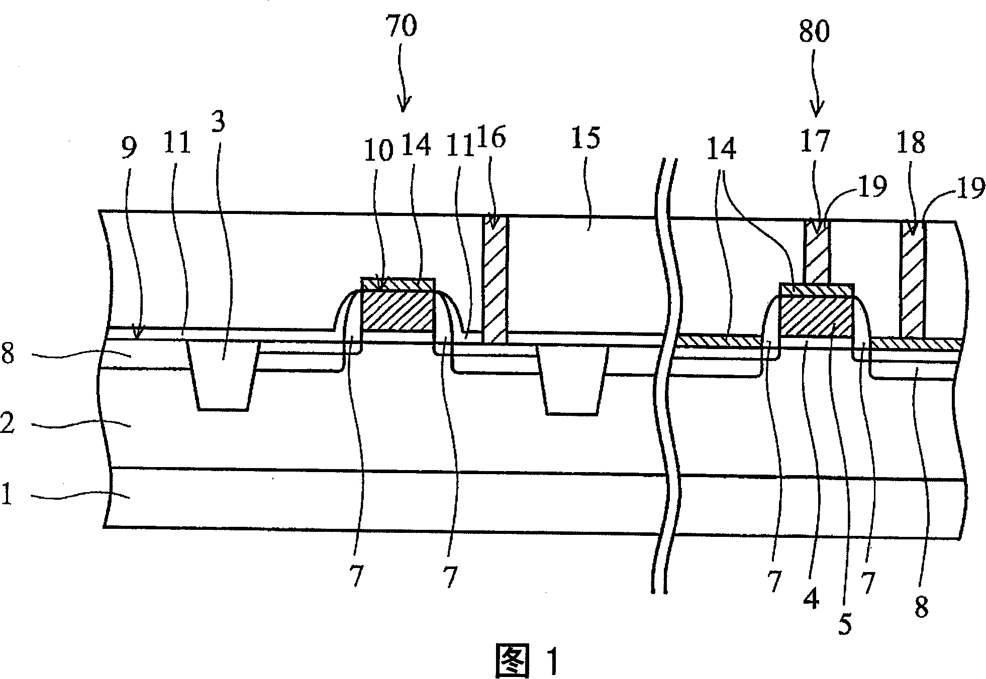
[0050] The invention provides a CMOS image display device, including forming salicide on the CMOS logic circuit area, and completely not forming metal silicide on the surface of the conversion transistor and the pinning photodiode. Below for the embodiment of the present invention, describe in detail as follows:

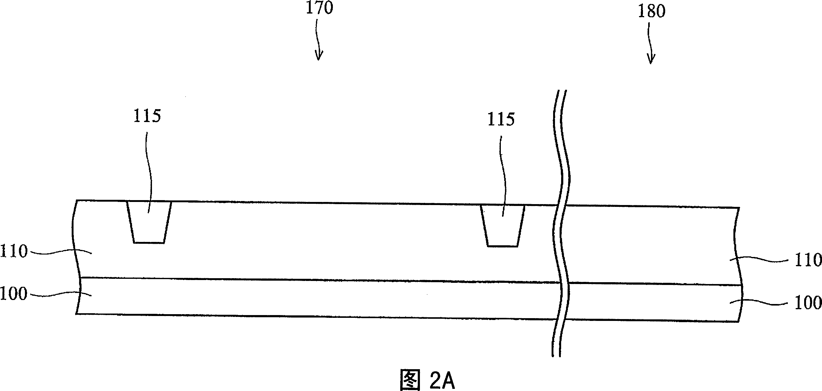
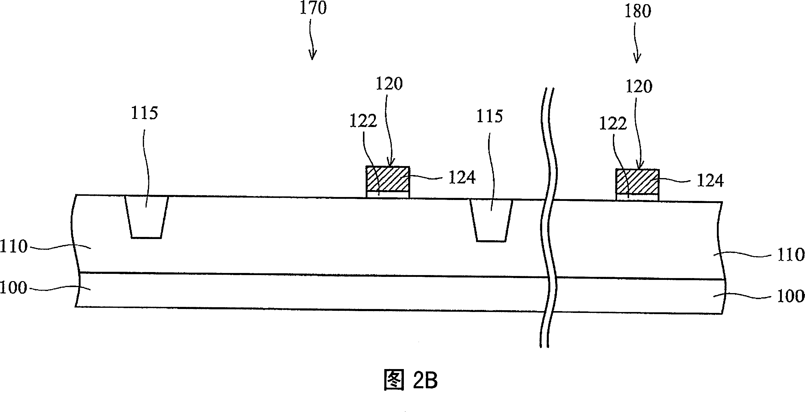
[0051] 2A-2F are schematic cross-sectional views showing various process steps of a CMOS image display device according to an embodiment of the present invention. In FIGS. 2A-2F , it is disclosed in detail that in the CMOS image display device, a salicide is formed on the CMOS logic circuit area at the same time, and no metal silicide is formed on the surface of the conversion transistor and the pinned photodiode at all.

[0052] Referring to FIG. 2A , a semiconductor substrate 100 is provided, such as a P-type single crystal silicon substrate with a crystal orientation. The semiconductor substrate 100 includes a first region 170 for forming image sensing pixels or...


PUM


Abstract

The present invention provides an image sensor device and photoelectric element. The image sensor device includes a first area with image sensing pixel array disposed on the underlay, and a second area with a logic circuit disposed on the underlay, wherein the logic circuit includes CMOS transistor. Each image sensing pixel includes transistor without self-aligned silicide and pinning photodiode. The CMOS transistor of the second area has self-aligned silicide, but the transistor of the first area has no self-aligned silicide. The present invention forms no metal silicide on the surface of the image sensing pixel area, thereby reduce the dark current effectively and further get an image sensor device with high signal-noise ratio. On the other hand, only forming the metal silicide on the top of the gate structure of the CMOS logic circuit area and the surface of the source / drain area, so the computing rate for the CMOS logic circuit is improved remarkably.

Description

technical field [0001] The present invention relates to an image sensor device, in particular to a complementary metal oxide semiconductor (CMOS) field effect transistor image sensor and an optoelectronic device. Background technique [0002] Complementary metal-oxide-semiconductor field-effect transistor image sensors (CMOS image sensors) have been widely used in many application fields, including, for example, digital still cameras (digital still cameras, DSCs) and camera phones. The above application fields mainly utilize an active pixel array or an image sensor cell array including photodiode elements to convert incident image light energy into digital information. [0003] As far as the field of still digital cameras is concerned, the performance requirements for image sensing mainly include high image quality and low crosstalk and noise, and can provide high-quality images under low ambient light conditions. [0004] A conventional image sensing unit includes an activ...

Claims


Application Information

Patent Timeline
Patent Type & Authority Applications(China)
IPC IPC(8): H01L27/146H04N5/30
CPCH01L27/14603H01L27/14643H01L27/14689H01L27/14609
Inventor 林志旻
Owner TAIWAN SEMICON MFG CO LTD
Why Eureka
Try Eureka