

Method of manufacturing flash memory device
A technology of flash memory devices and high-voltage transistors, which is applied in semiconductor/solid-state device manufacturing, electrical components, circuits, etc., and can solve problems such as unit size reduction and quasi-margin reduction
- Summary
- Abstract
- Description
- Claims
- Application Information
AI Technical Summary
Problems solved by technology
Method used
Image

Examples
Embodiment Construction
[0029] The present invention will be described below in conjunction with specific exemplary embodiments with reference to the accompanying drawings.
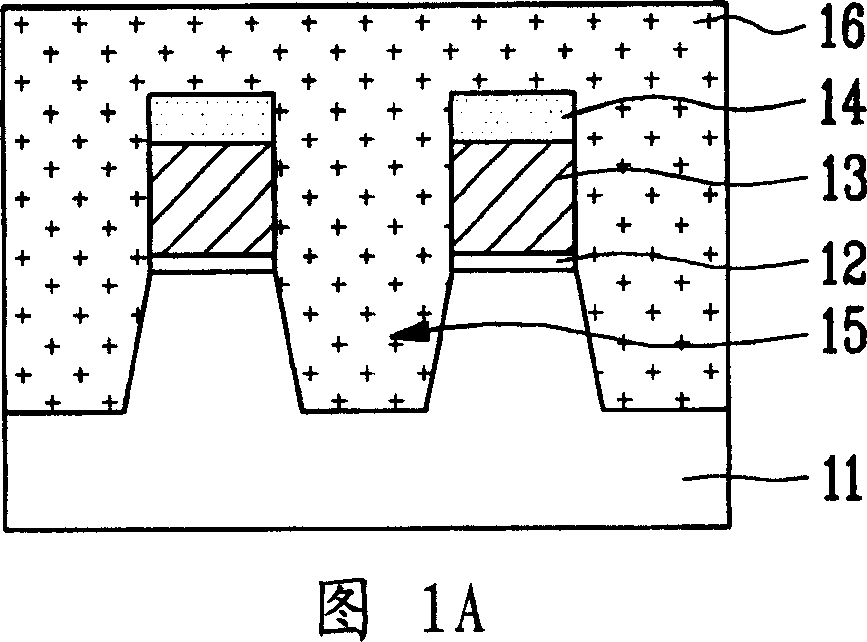
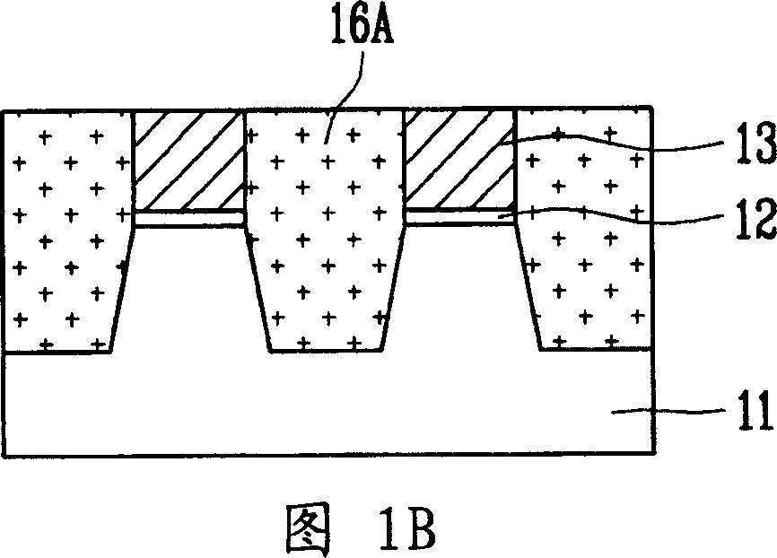
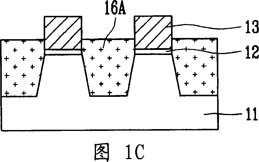
[0030] 1A to 1D are cross-sectional views illustrating a method of manufacturing a flash memory device according to a first embodiment of the present invention.
[0031] Referring to FIG. 1A , a tunnel oxide film 12 , a first conductive layer 13 and a hard mask film 14 are sequentially formed on a semiconductor substrate 11 . The first conductive layer 13 may preferably be formed to a thickness of 700 Ȧ to 1500 Ȧ in order to prevent warping of the tunnel oxide film 12 by sequentially laminating an undoped polysilicon film and a doped polysilicon film. The undoped polysilicon film may be formed to have a thickness that is half or less of the total thickness of the first conductive layer 13 . Meanwhile, when the first conductive layer 13 is applied to a single layer unit, it may preferably be formed in a thickness of 1000 Ȧ to 15...
PUM
 Abstract
Description
Claims
Application Information