Plasma stability determination method and plasma processing apparatus

a stability determination and plasma technology, applied in plasma techniques, semiconductor/solid-state device testing/measurement, electric discharge tubes, etc., can solve the problems of deterioration of the uniformity of plasma processing in the plane of the wafer, the above-mentioned parameter may frequently or largely fluctuate, etc., to achieve the effect of properly determining the stability of the plasma

Active Publication Date: 2018-09-11
TOKYO ELECTRON LTD
View PDF3 Cites 0 Cited by
  • Summary
  • Abstract
  • Description
  • Claims
  • Application Information

AI Technical Summary

Benefits of technology

[0015]According to the present disclosure, it is possible to properly determine the stability of the plasma in the plasma processing apparatus.

Problems solved by technology

However, when an abnormal discharge occurs due to a certain factor in the plasma processing, in other words, when the plasma in the processing container becomes unstable, the above-mentioned parameter may frequently or largely fluctuate.
In such a case, the stability of the plasma processing may not be ensured.
Thus, the uniformity of the plasma processing in the plane of the wafer is deteriorated.
As a result, some defects may occur on the wafer.
However, the present inventors have found that, in the method of Patent Document 1, a defect is generated in the wafer, even though the fluctuation range of the parameter falls within the reference value.
In the case where the parameters fluctuate, it is presumed that the cause of the defect is that plasma cannot be stably generated in the processing container, thereby deteriorating the uniformity of the plasma processing in the plane of the wafer.
In addition, for example, in a case where the abnormality cannot be detected by the method of Patent Document 1, the plasma processing may be continued in a state where the plasma is not stable, so that a large number of defective wafers are produced until the abnormality is found in the subsequent defect inspection step.

Method used


Image

  • Plasma stability determination method and plasma processing apparatus
  • Plasma stability determination method and plasma processing apparatus
  • Plasma stability determination method and plasma processing apparatus

Examples


Embodiment Construction

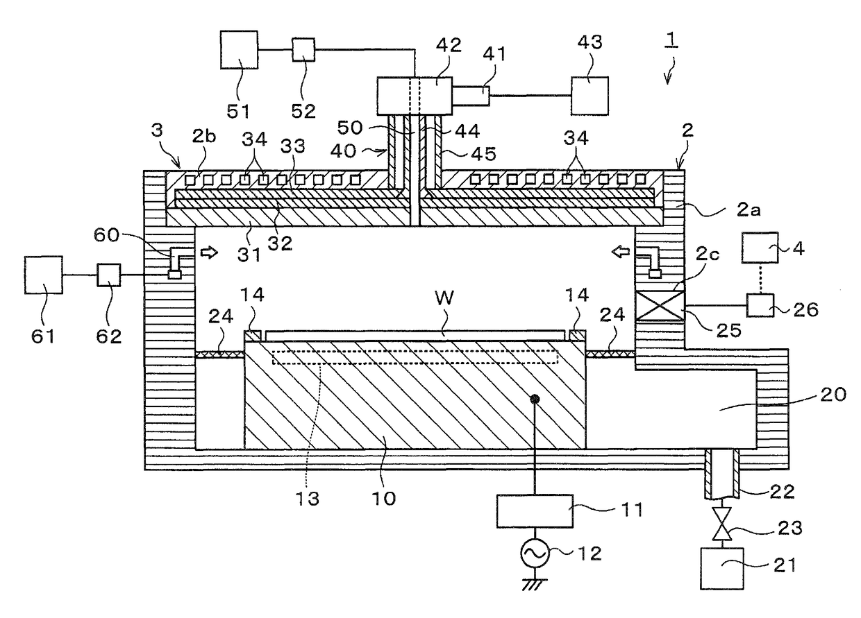
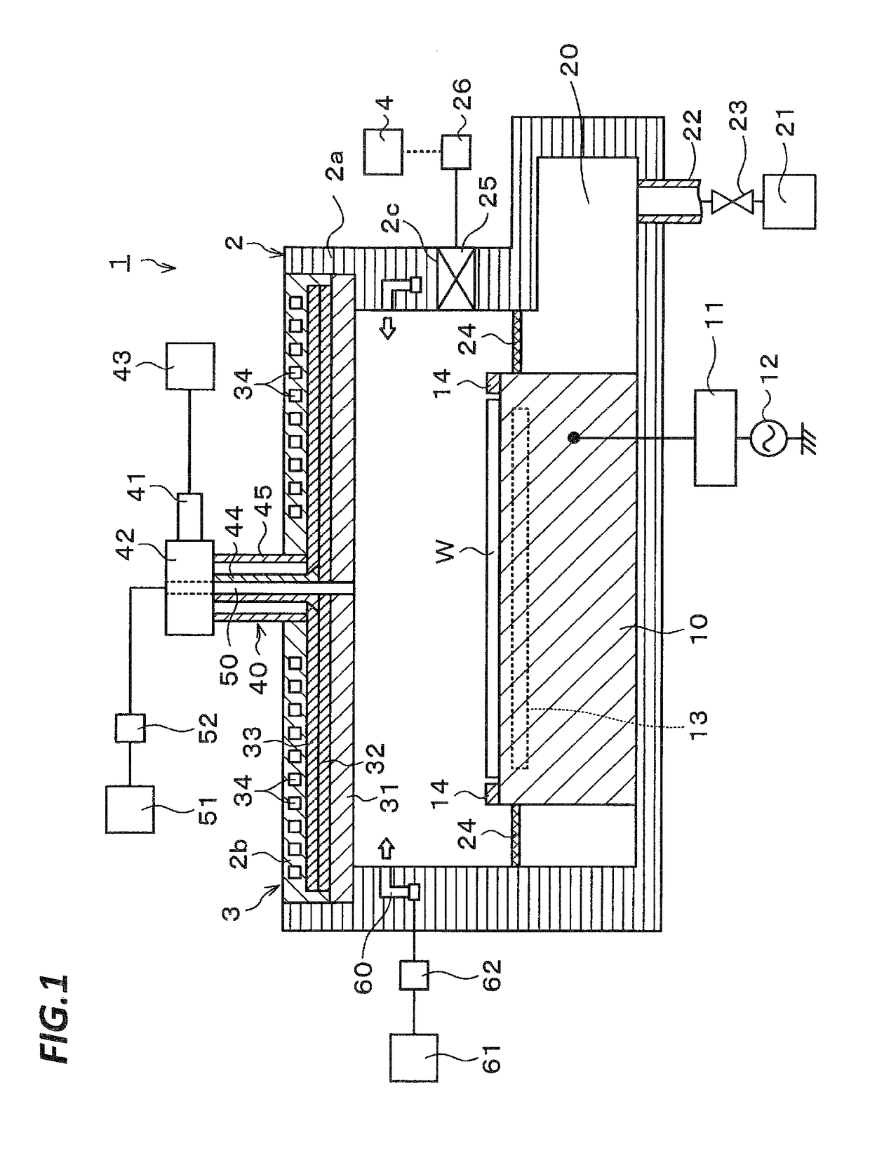
[0024]Hereinafter, an exemplary embodiment of the present disclosure will be described. FIG. 1 is a vertical-sectional view illustrating a schematic configuration of a plasma processing apparatus 1 according to an exemplary embodiment of the present disclosure. In the exemplary embodiment, descriptions will be made on a case where the stability of plasma in the plasma processing apparatus 1 is determined when a resist film formed on the surface of a wafer W is etched by a plasma processing using, for example, an oxygen-containing gas and a fluorine-containing gas. In the present specification and drawings, components having substantially the same functional configurations will be denoted by the same symbols, and the overlapping descriptions thereof will be omitted.

[0025]The plasma processing apparatus 1 includes a processing container 2 of which the inside is hermetically maintained, a radial line slot antenna 3 that supplies microwaves for plasma generation into the processing cont...


PUM


Abstract

A method and apparatus for determining a stability of plasma in a plasma processing apparatus for performing a plasma processing by converting into plasma a processing gas supplied into a processing container. The method includes: detecting a light emission intensity of the plasma in the processing container while the plasma is generated in the processing container; generating a first function representing a relationship between time and the light emission intensity from a detection result of the light emission intensity; differentiating the first function with time to calculate a differential value, and generating a second function from a relationship between an absolute value of the differential value and time; and integrating the second function with time to calculate an integral value, and determining a stability of the plasma based on the calculated integral value. A related apparatus is also provided.

Description

CROSS-REFERENCE TO RELATED APPLICATIONS[0001]This application is a 35 U.S.C. 371 National Phase Entry Application from PCT / JP2015 / 069521, filed Jul. 7, 2015, which claims priority from Japanese Patent Application No. 2014-160542 filed on Aug. 6, 2014 with the Japan Patent Office, the disclosure of which are incorporated herein in their entirety by reference.TECHNICAL FIELD[0002]The present disclosure relates to a method for determining a stability of plasma in a plasma processing apparatus for performing a processing on a workpiece by converting a processing gas supplied into a processing container into plasma, and a plasma processing apparatus.BACKGROUND[0003]In manufacturing a semiconductor device, a film forming processing or an etching processing is performed using a plasma processing apparatus on a semiconductor wafer (hereinafter, simply referred to as a “wafer”) as a workpiece. In the film forming processing or the etching processing, a gas is introduced into a vacuum process...

Claims


Application Information

Patent Timeline
Patent Type & Authority Patents(United States)
IPC IPC(8): H01L21/00H01L21/3065H05H1/00H05H1/46H01L21/66H01L21/67
CPCH01L21/67253H01L21/3065H01L21/67069H05H1/0025H05H1/46H01L22/10H05H2001/463H01J37/32935H01J37/32972H05H1/463
Inventor MIYAMA, RYOWATANABE, NAOTONAKAMURA, KOICHIRO
Owner TOKYO ELECTRON LTD
Why Eureka
Try Eureka