Optical modulator

a phase shifter and optical modulator technology, applied in non-linear optics, instruments, optics, etc., can solve the problems of less favorable f metric and consume a minimal amount of die area, and achieve the effect of enhancing overlap

Active Publication Date: 2018-11-06
NOKIA SOLUTIONS & NETWORKS OY
View PDF15 Cites 5 Cited by
  • Summary
  • Abstract
  • Description
  • Claims
  • Application Information

AI Technical Summary

Benefits of technology

[0008]An aspect of the present disclosure relates to an optical modulator semiconductor device comprising an optical waveguide. The optical waveguide comprises a p-type region of semiconductor material and an n-type region of semiconductor material, the n-type region and the p-type region sharing a non-planar junction interface configured to increase a junction area between the n-type region and the p-type region per unit length of the optical waveguide so as to enhance an overlap between an optical mode in the optical waveguide and the junction area. The non-planar junction interface comprises a curved surface having a convex side and a concave side. In some implementations the p-type region is on the concave side of the non-planar junction interface and the n-type region is on the convex side of the non-planar junction interface. In some implementations the n-type region is on the concave side of the non-planar junction interface and the p-type region is on the convex side of the non-planar junction interface. In some implementations the p-type region is on the concave side of the non-planar junction interface at one location along the length of the optical waveguide, and is on the convex side of the non-planar junction interface at another location along the length of the optical waveguide.
[0012]Another aspect of the present disclosure relates to a method of fabricating an optical modulator comprising: a) providing a semiconductor material upon a planar substrate; and, b) forming an optical waveguide with the semiconductor material, the optical waveguide comprising a p-type region and an n-type region defined therein so that at least one of the p-type region and the n-type region comprises a protrusion region interposed between portions of the other of the p-type region and the n-type region in a height dimension normal to the substrate, said protrusion region defining a non-planar junction interface between the n-type and p-type regions for enhancing an overlap between an optical mode of the optical waveguide and the non-planar junction interface.
[0018]Another aspect of the present disclosure relates to a method of fabricating an optical modulator semiconductor device using the steps of: providing a semiconductor material in planar form; forming a slab waveguide structure from the semiconductor material by an anisotropic etch; depositing a thin layer of an insulator conformally on top of the slab waveguide; implanting n-type and p-type dopants into the slab waveguide in multiple implantation steps to produce n-type and p-type regions, respectively; and annealing the implanted slab waveguide structure; thereby forming within the slab waveguide structure a p-type region and an n-type region, the n-type region and the p-type region having a non-planar junction interface having a length dimension, the non-planar common junction configured to increase a junction area between the n-type region and the p-type region per unit length of the length dimension of the junction, so as to so as to enhance an overlap between an optical mode in the optical waveguide and the junction area when the optical modulator semiconductor device is operational.

Problems solved by technology

However, for silicon photonics technology to be widely adopted, a key challenge that needs to be addressed is achieving efficient and high-speed modulation in silicon, while consuming a minimal amount of die area.
Simply raising the dopant concentrations will actually lead to a less favorable F metric.
These are promising results, but to achieve this ultra low VπL, a 200 nm inter-digitation period is required; this will present difficulties as currently most silicon photonics implant layers are fabricated with lower-resolution masks.

Method used


Image

  • Optical modulator
  • Optical modulator
  • Optical modulator

Examples


application examples

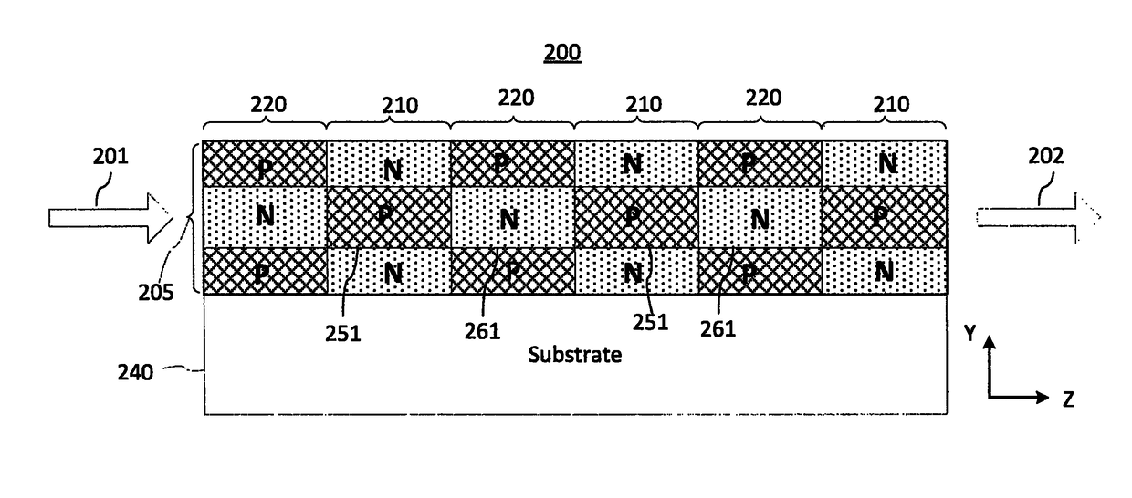
[0099]FIG. 5A is an illustration of a Mach Zehnder interferometer built using devices fabricated according to principles of the invention. In FIG. 5A a Mach Zehnder interferometer (MZI) modulator using the described phase shifter has a light input (optical input 510) from the left waveguide and an output (optical output 530) from the right. The phase shifters 520 are loaded on both arms.

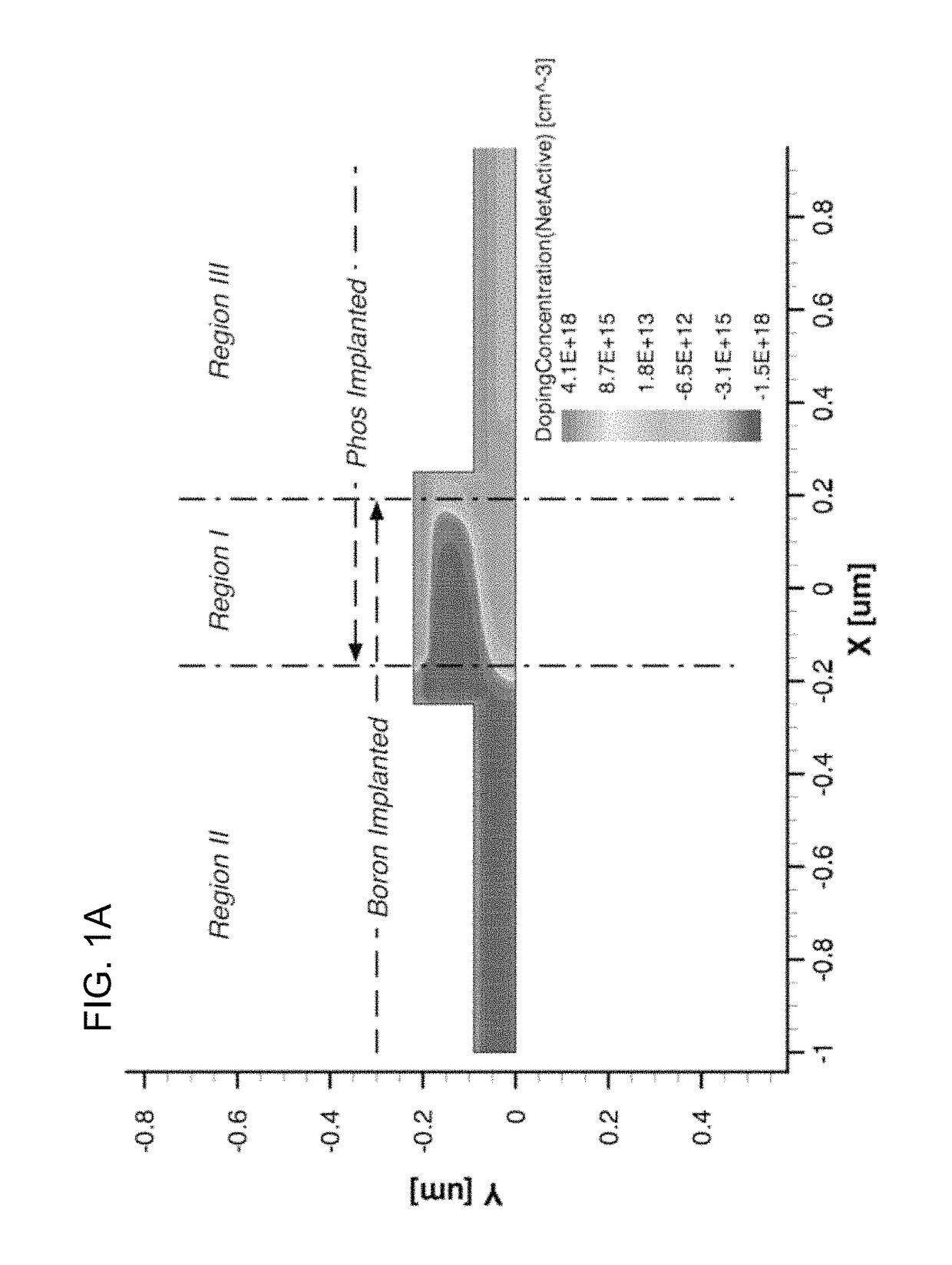
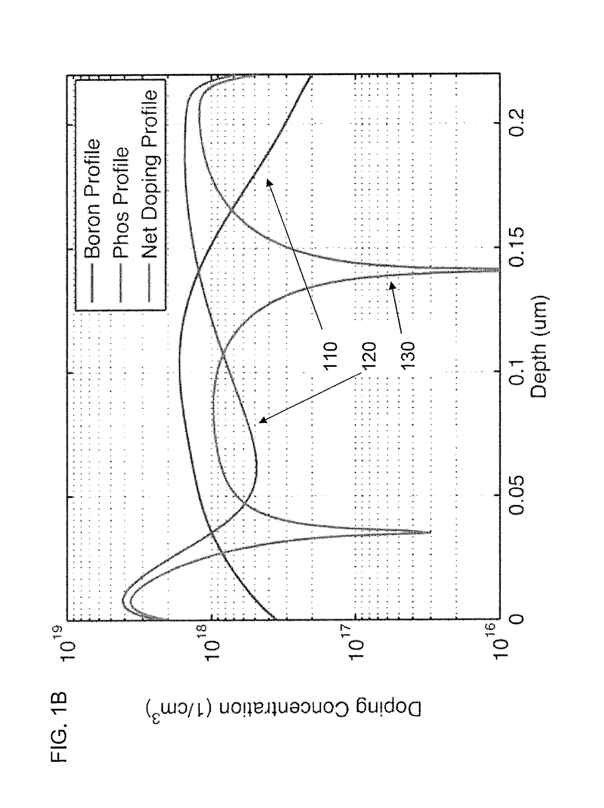
[0100]FIG. 5B is a diagram illustrating the detailed doping mask for the phase shifter, in which N and P implantations overlap in the center of the waveguide.

[0101]FIG. 5C is a diagram illustrating a more detailed view of a portion of the doping mask in FIG. 5B.

[0102]FIG. 5D is a diagram illustrating the dimensions of layers in the center of the waveguide. The dimensions presented in the diagrams are typical dimensions in a preferred embodiment.

[0103]FIG. 6 is an illustration of a ring modulator constructed using devices fabricated according to principles of the invention. In FIG. 6 there are shown e...


PUM

PropertyMeasurementUnit
free-space wavelengthsaaaaaaaaaa
widthaaaaaaaaaa

Abstract

A novel phase shifter design for carrier depletion based silicon modulators, based on an experimentally validated model, is described. It is believed that the heretofore neglected effect of incomplete ionization will have a significant impact on ultra-responsive phase shifters. A low VπL product of 0.3V·cm associated with a low propagation loss of 20 dB / cm is expected to be observed. The phase shifter is based on overlapping implantation steps, where the doses and energies are carefully chosen to utilize counter-doping to produce an S-shaped junction. This junction has a particularly attractive VπL figure of merit, while simultaneously achieving attractively low capacitance and optical loss. This improvement will enable significantly smaller Mach-Zehnder modulators to be constructed that nonetheless would have low drive voltages, with substantial decreases in insertion loss. The described fabrication process is of minimal complexity; in particular, no high-resolution lithographic step is required.

Description

CROSS-REFERENCE TO RELATED APPLICATIONS[0001]This application is a continuation-in-part of pending U.S. patent application Ser. No. 15 / 481,669, filed on Apr. 7, 2017, titled “ULTRA-RESPONSIVE PHASE SHIFTERS FOR DEPLETION MODE SILICON MODULATORS”, which is a continuation of U.S. patent application Ser. No. 14 / 840,409, filed Aug. 31, 2015, now U.S. Pat. No. 9,638,942, which is a continuation of U.S. patent application Ser. No. 14 / 060,058 filed on Oct. 22, 2013, now U.S. Pat. No. 9,158,138, which claimed the priority to and the benefit of then U.S. provisional patent application Ser. No. 61 / 823,344, filed May 14, 2013, each of which applications is incorporated herein by reference in its entirety.FIELD OF THE INVENTION[0002]The invention relates to phase shifters in general and particularly to optical phase shifters and optical modulators utilizing semiconductor PN junctions.BACKGROUND OF THE INVENTION[0003]In the past decade, there has been a rapidly growing need for communication ban...

Claims


Application Information

Patent Timeline
Patent Type & Authority Patents(United States)
IPC IPC(8): G02F1/035G02F1/015G02F1/025G02F1/225G02F1/01
CPCG02F1/025G02F1/015G02F1/2257G02F1/01G02F2001/0152G02F1/035G02F1/0353G02F1/0356G02F2001/0113G02F1/011G02F1/0152G02F1/0113
Inventor BAEHR-JONES, THOMASLIU, YANG
Owner NOKIA SOLUTIONS & NETWORKS OY
Why Eureka
Try Eureka