
Centralized built-in soft-repair architecture for integrated circuits with embedded memories

a technology of embedded memory and soft-repair architecture, which is applied in the direction of fault response, error detection/correction, instruments, etc., can solve the problems of large chip area in the soc that is also the most vulnerable to manufacturing defects, and the embedded memory is not accessible over the system bus, so as to achieve efficient results

Active Publication Date: 2018-11-20
TEXAS INSTR INC
View PDF12 Cites 6 Cited by
  • Summary
  • Abstract
  • Description
  • Claims
  • Application Information

AI Technical Summary

Benefits of technology

[0018]Disclosed embodiments provide built-in self-repair circuitry and a method of operating the same that can be efficiently realized in a large-scale integrated circuit.
[0020]Disclosed embodiments provide such circuitry and method that reduces the test time required for executing built-in self-repair.
[0021]Disclosed embodiments provide such circuitry and method that reduces power consumption in the built-in self-repair circuitry during normal operation.

Problems solved by technology

In many instances, these embedded memories are not accessible over the system bus, but are only available to the processor circuitry in which it is realized.
Some conventional BIST memory test techniques include the placement of hardwired logic in the SoC, by way of which memory test algorithms developed at the time of circuit design are implemented; however, it may not be feasible to determine the particular tests to be performed at that early stage of the process.
Accordingly, a large portion of the chip area in the SoC will also be the most vulnerable to manufacturing defects.
Given these techniques, hard repair is best-suited for configuring memory redundancy at manufacturing test, but generally cannot be invoked for repairing later-life failed bits.
Conversely, soft repair can be used at the time of manufacture and also over the device life, but requires complete testing of the memories, and repeating of the memory test following the loading of the repair configuration, each time that the device is powered up.
This diversity in embedded memory type and BIST datapath architecture greatly complicates the implementation of BISR to maximize manufacturing yield and maintain reliability of the overall device.
Those SoC devices that include processor cores from different sources or vendors complicate the BISR task.
However, memory controller functions within these “black box” processor core IPs apply banking and other logical address translation to the embedded memories, such that full control of the addressing and operation of the embedded memories is not available to BIST and BISR circuitry outside of those IPs.
In some conventional SoC implementations, BISR is simply not available for memories embedded in these black box processor cores.
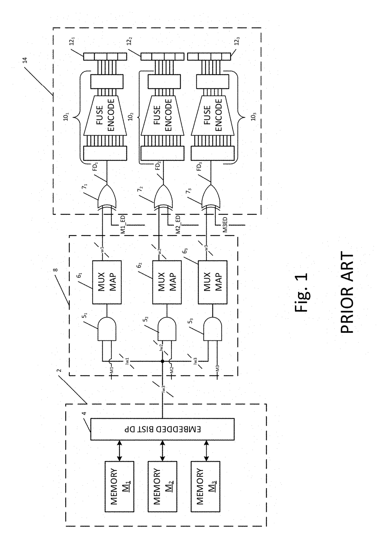
The chip area required under this approach can be quite substantial, and thus costly to implement in terms of silicon real estate.
Especially in SoC devices with diverse processor cores (i.e., some including embedded BIST circuitry), this approach is very area intensive, and thus costly to implement in modern large scale integrated circuits.
Considering that many modern SoC devices include hundreds of embedded memories, the chip area overhead necessary for self-test and self-repair logic can be massive, in some cases requiring as many as one million logic gates.
This overhead will appear especially costly for mature devices, since the utilization of the available fuses in the fuse ROM will be relatively low for high-yield devices, yet the BISR circuitry must yet be present.

Method used


Image

  • Centralized built-in soft-repair architecture for integrated circuits with embedded memories
  • Centralized built-in soft-repair architecture for integrated circuits with embedded memories
  • Centralized built-in soft-repair architecture for integrated circuits with embedded memories

Examples


Embodiment Construction

[0033]The one or more embodiments described in this specification are implemented into a multiple-core large-scale integrated circuit, such as that suitable as a system-on-a-chip (SoC) or similar device, as it is contemplated that such implementation is particularly advantageous in that context. However, it is also contemplated that concepts of this invention may be beneficially applied to other applications, including general purpose microprocessors, application specific processors, and the like. Accordingly, it is to be understood that the following description is provided by way of example only, and is not intended to limit the true scope of this invention as claimed.

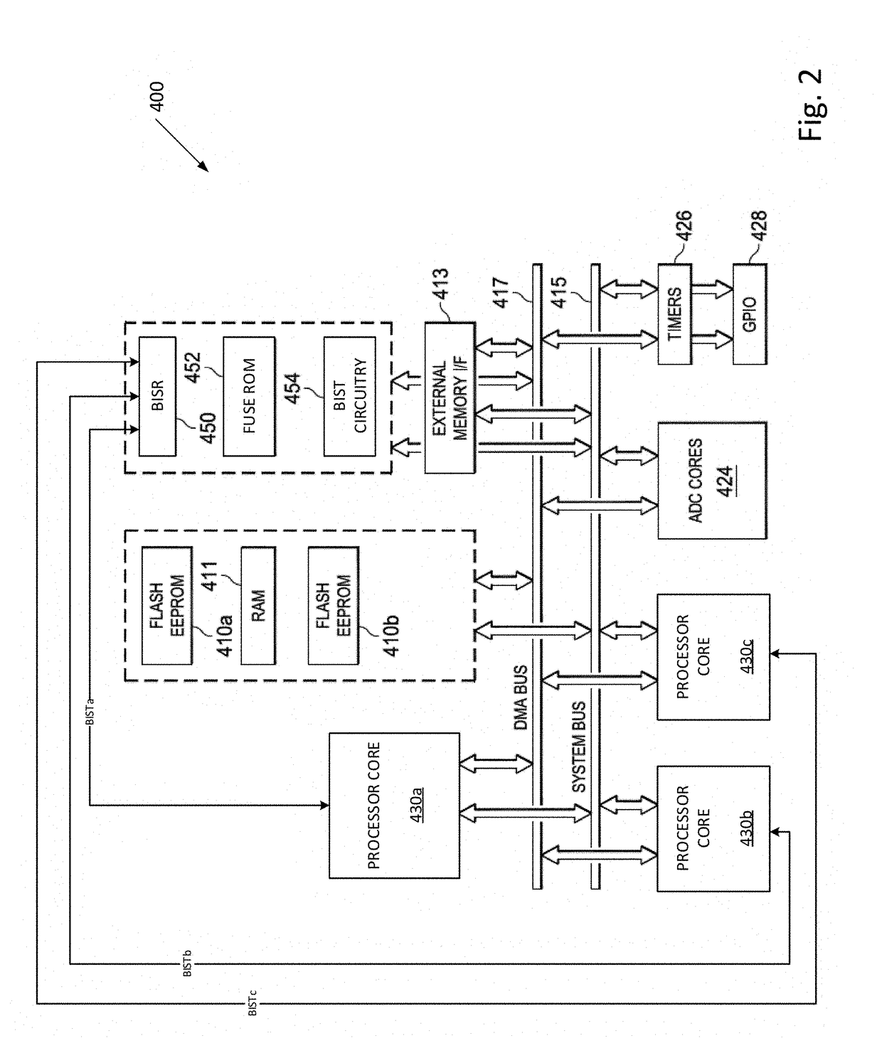
[0034]FIG. 2 illustrates, in block diagram form, the generalized architecture of an example of SoC 400 constructed according to these embodiments. In this example, SoC 400 as shown in FIG. 2 follows the generalized architecture of a modern system-on-a-chip such as in the TDAxx and DRAx families of processors availabl...


PUM


Abstract

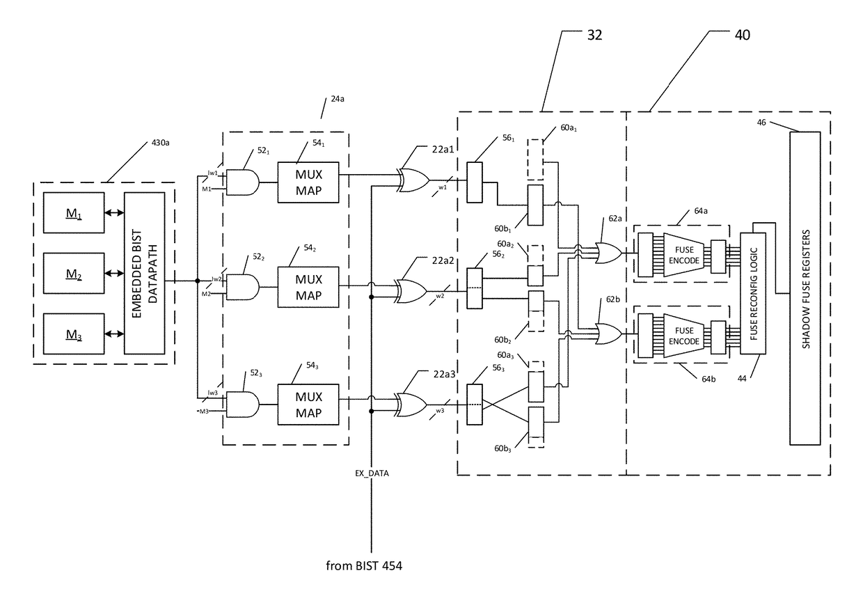
A large-scale integrated circuit with built-in self-repair (BISR) circuitry for enabling redundancy repair for embedded memories in each of a plurality of processor cores with embedded built-in self-test (BIST) circuitry. The BISR circuitry receives and decodes BIST data from the embedded memories into fail signature data in a physical-aware form on which repair analysis can be performed. The fail signature data is reformatted into a unified repair format, such that a fuse encoder circuit can be used to encode fuse patterns in that unified repair format for a repair entity for each of the embedded memories. The fuse patterns are reconfigured into the appropriate order for storing in shadow fuse registers associated with the specific embedded memories.

Description

CROSS-REFERENCE TO RELATED APPLICATIONS[0001]This application claims priority, under 35 U.S.C. § 119(e), of Provisional Application No. 62 / 272,518, filed Dec. 29, 2015, incorporated herein by this reference.STATEMENT REGARDING FEDERALLY SPONSORED RESEARCH OR DEVELOPMENT[0002]Not applicable.BACKGROUND OF THE INVENTION[0003]This invention is in the field of the test and configuration of large scale integrated circuits. Embodiments are more specifically directed to an architecture for invoking redundant memory elements.[0004]Many modern electronic integrated circuits integrate essentially all necessary functional components of a computer system, whether general purpose or arranged for a particular end application. Those large scale integrated circuits that include the computational capability for controlling and managing a wide range of functions and useful applications are often referred to as “system on a chip”, or “SoC”, devices. Typical modern SoC architectures include one or more ...

Claims


Application Information

Patent Timeline
Patent Type & Authority Patents(United States)
IPC IPC(8): G11C29/44G06F11/20G11C29/00G11C29/12G01R31/28
CPCG11C29/4401G06F11/2017G11C29/12G11C29/44G11C29/702G11C29/72G11C29/787G11C29/838G11C29/70G01R31/2851G11C2029/0401G06F11/14
Inventor VARADARAJAN, DEVANATHANKALE, SUMANT DINKAR
Owner TEXAS INSTR INC
Learn More