Eureka AIR delivers breakthrough ideas for toughest innovation challenges, trusted by R&D personnel around the world.

Methods for anisotropic control of selective silicon removal

a selective silicon and anisotropic control technology, applied in the field of semiconductor processing, can solve the problems of unplanned etching of the second material, and achieve the effects of reducing the possibility of overhang, reducing unwanted etching, and improving the performance and reliability of the semiconductor devi

Active Publication Date: 2019-01-01
APPLIED MATERIALS INC
View PDF1917 Cites 3 Cited by
  • Summary
  • Abstract
  • Description
  • Claims
  • Application Information

AI Technical Summary

Benefits of technology

The present technology may improve the performance and reliability of semiconductor devices by reducing unwanted etching near critical features. This is done by partially or fully blocking etchants from reaching the bottom of a trench or via, which results in an anisotropic etch. Additionally, it may reduce the possibility of overhang at the top of a trench or via by preferentially etching the top of the trench or via.

Problems solved by technology

However, even though an etch process may be selective to a first material over a second material, some undesired etching of the second material may still occur.

Method used


Image

  • Methods for anisotropic control of selective silicon removal
  • Methods for anisotropic control of selective silicon removal
  • Methods for anisotropic control of selective silicon removal

Examples


Embodiment Construction

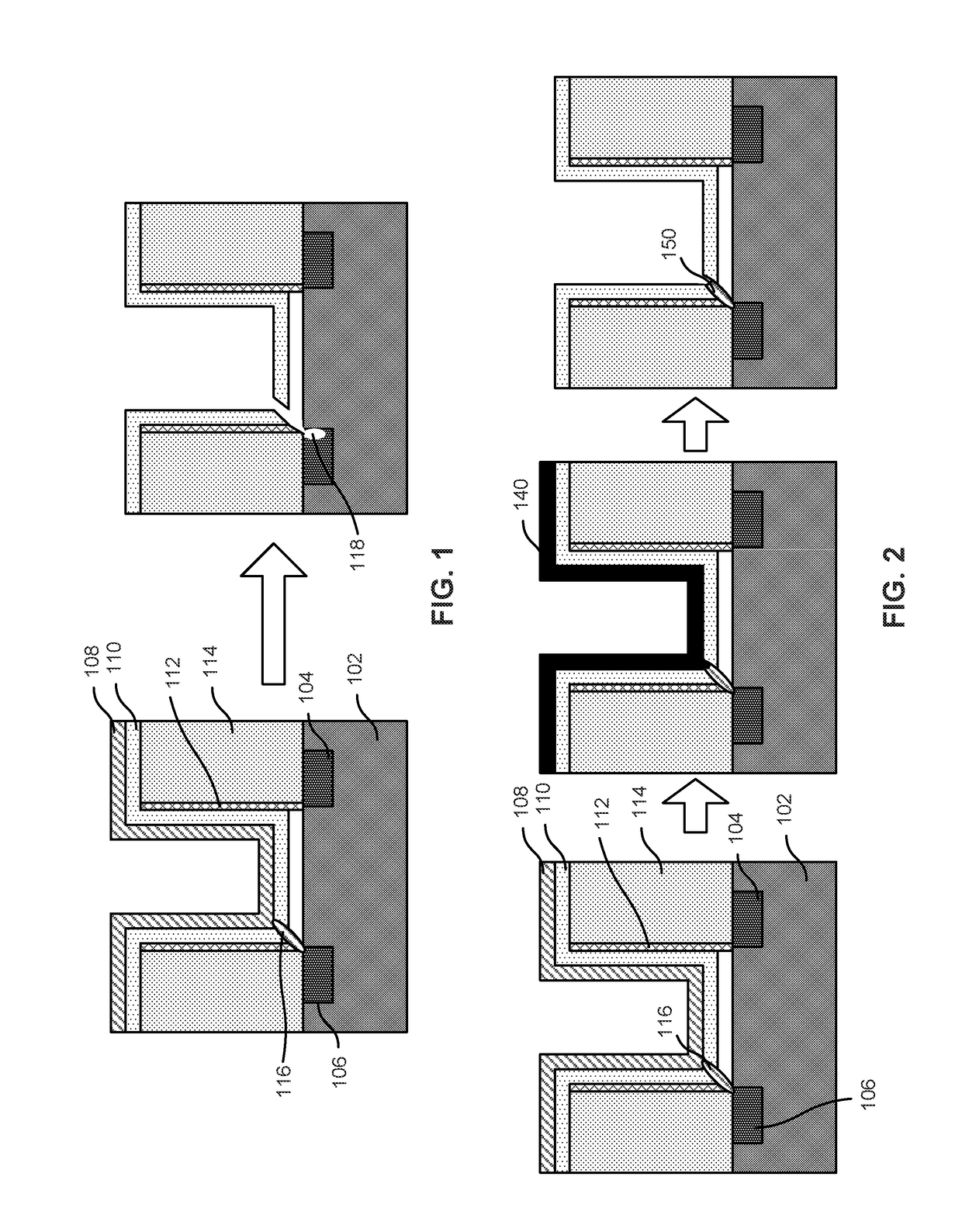
[0017]As characteristic dimensions decrease, the negative effects of process defects on performance and reliability increases. For example, FIG. 1 shows that a conventional process may result in a leakage path. Substrate 102 has electrically active areas 104 and 106. Substrate 102 may be a silicon wafer, and electrically active areas 104 and 106 may include silicon germanium and / or silicon phosphorous. A trench is defined by a polysilicon cap 108 on a high-k dielectric layer 110. The high-k dielectric layer may be adjacent to a spacer 112, which may be adjacent to layer 114. A processing defect may be present in the bottom of the trench, which may cause an undesired deposit 116 of polysilicon. In a conventional etch of polysilicon, polysilicon cap 108 may be etched away. However, undesired deposit 116 may also be etched, which may lead to parts of electrically active area 106 being etched away, resulting in void 118. Void 118 may cause poor device performance including shorting or n...


PUM


Abstract

Embodiments of the present technology may include a method of etching. The method may include flowing a gas through a plasma to form plasma effluents. The method may also include reacting plasma effluents with a first layer defining a first feature. The first feature may include a first sidewall, a second sidewall, and a bottom. The first sidewall, the second sidewall, and the bottom may include the first layer. The first layer may be characterized by a first thickness on the sidewall. The method may further include forming a second layer from the reaction of the plasma effluents with the first layer. The first layer may be replaced by the second layer. The second layer may be characterized by a second thickness. The second thickness may be greater than or equal to the first thickness. The method may also include removing the second layer to expose a third layer.

Description

TECHNICAL FIELD[0001]The present disclosure applies broadly to the field of semiconductor processing. More specifically, methods for radical etching of layers are disclosed.BACKGROUND[0002]Integrated circuits are made possible by processes which produce intricately patterned material layers on substrate surfaces. Producing patterned material on a substrate requires controlled methods for removal of exposed material. Chemical etching is used for a variety of purposes including transferring a pattern in photoresist into underlying layers, thinning layers, or thinning lateral dimensions of features already present on the surface. Often it is desirable to have an etch process that etches one material faster than another facilitating, for example, a pattern transfer process. Such an etch process is said to be selective to the first material. As a result of the diversity of materials, circuits, and processes, etch processes have been developed with a selectivity towards a variety of mater...

Claims


Application Information

Patent Timeline
Patent Type & Authority Patents(United States)
IPC IPC(8): H01L21/302H01L29/66H01L21/3065H01L21/3213H01L21/02H01L29/40H01L21/67H01L21/311
CPCH01L21/32137H01L21/3065H01L29/66545H01L21/02252H01L21/67069H01L21/02123H01L29/401H01L21/31138H01L21/31116H01J37/32357H01J37/32422H01J37/3244
Inventor LI, ZIHUIKAO, CHIA-LINGWANG, ANCHUANINGLE, NITIN K.
Owner APPLIED MATERIALS INC
Why Eureka
Eureka Blog
Learn More