Method of forming high dielectric constant dielectric layer by atomic layer deposition

Active Publication Date: 2019-02-12
UNITED MICROELECTRONICS CORP
View PDF6 Cites 157 Cited by
  • Summary
  • Abstract
  • Description
  • Claims
  • Application Information

AI Technical Summary

Benefits of technology

[0003]A method of forming a high dielectric constant (high-k) dielectric layer by atomic layer deposition is provided in the present invention. A first oxygen precursor pulse, a first oxygen precursor purge, a chemical precursor pulse, and a chemical precursor purge are sequentially performed and are repeated by at least 3 cycles before a second oxygen precursor pulse and a second oxygen precursor purge for reducing impurities in the high dielectric constant dielectric layer.
[0004]A method of forming a high dielectric constant dielectric layer by atomic layer deposition includes the following steps. A plurality of cycles are performed one after another,

Problems solved by technology

As the thickness of the gate dielectric layer in the metal-oxide-semiconductor field effect transistor (MOSFET) decr

Method used


Image

  • Method of forming high dielectric constant dielectric layer by atomic layer deposition
  • Method of forming high dielectric constant dielectric layer by atomic layer deposition
  • Method of forming high dielectric constant dielectric layer by atomic layer deposition

Examples


Embodiment Construction

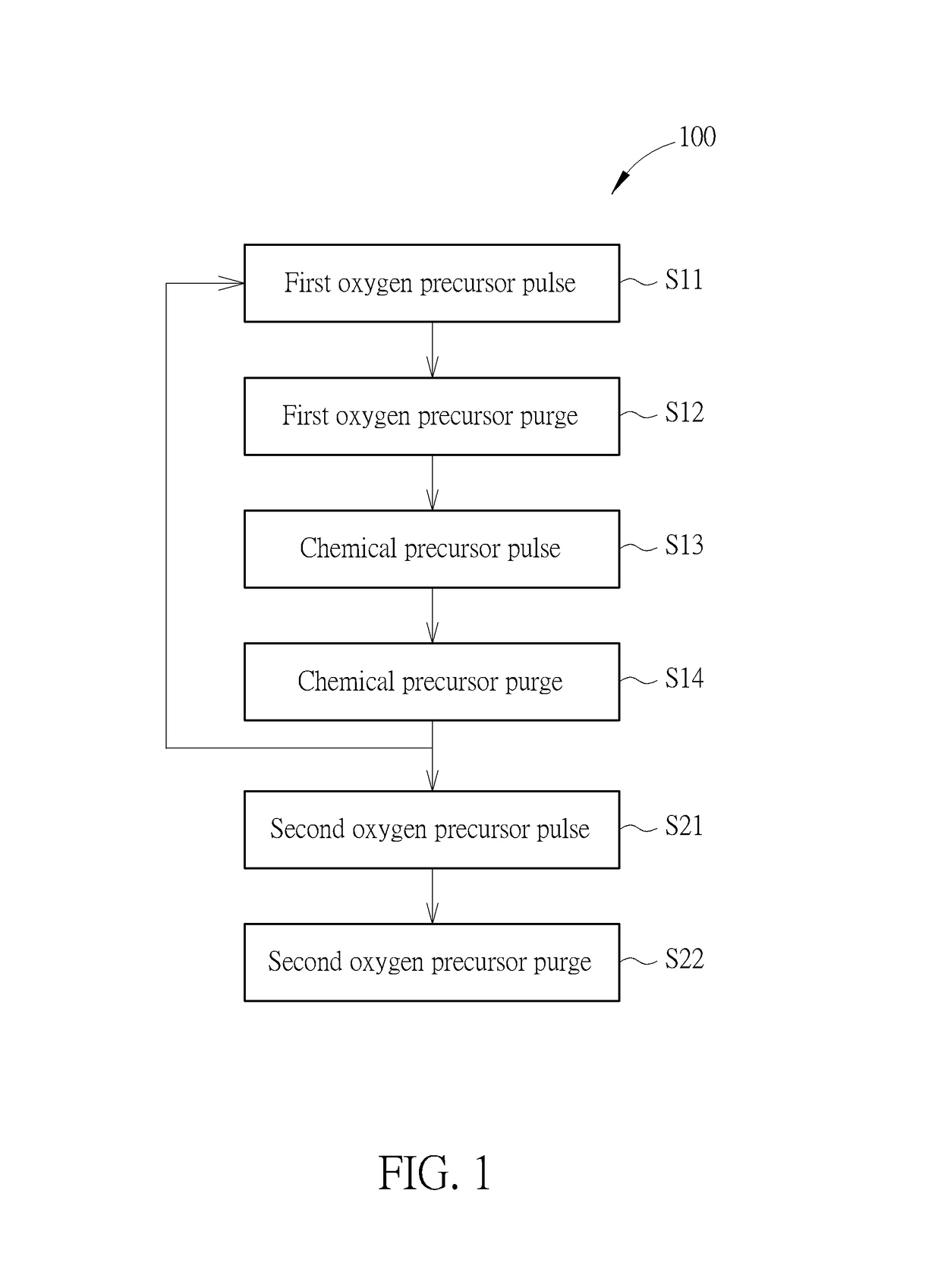
[0013]Please refer to FIGS. 1-8. FIG. 1 is a flow chart of a method of forming a high dielectric constant (high-k) dielectric layer by atomic layer deposition (ALD) according to an embodiment of the present invention. FIGS. 2-8 are schematic drawings illustrating the method of forming the high dielectric constant dielectric layer by atomic layer deposition in this embodiment. The method of forming the high dielectric constant dielectric layer by atomic layer deposition in this embodiment may include the following steps. As shown in FIG. 1 and FIG. 2, a plurality of cycles 100 are performed one after another, and each of the cycles 100 sequentially includes step S11, step S12, step S13, and step S14. In step S11, a first oxygen precursor pulse is performed to supply an oxygen precursor to a substrate 10 disposed in a reactor (not shown). In some embodiments, the reactor may be a process chamber of an ALD apparatus or other portion of the ALD apparatus, but not limited thereto. In som...


PUM

PropertyMeasurementUnit
Concentrationaaaaaaaaaa
Dielectric constantaaaaaaaaaa

Abstract

A method of forming a high dielectric constant (high-k) dielectric layer by atomic layer deposition includes the following steps. Cycles are performed one after another, and each of the cycles sequentially includes performing a first oxygen precursor pulse to supply an oxygen precursor to a substrate disposed in a reactor; performing a first oxygen precursor purge after the first oxygen precursor pulse; performing a chemical precursor pulse to supply a chemical precursor to the substrate after the first oxygen precursor purge; and performing a chemical precursor purge after the chemical precursor pulse. The first oxygen precursor pulse, the first oxygen precursor purge, the chemical precursor pulse, and the chemical precursor purge are repeated by at least 3 cycles. A second oxygen precursor pulse is performed to supply an oxygen precursor to the substrate after the cycles. A second oxygen precursor purge is performed after the second oxygen precursor pulse.

Description

BACKGROUND OF THE INVENTION1. Field of the Invention[0001]The present invention relates to a method of forming a high dielectric constant (high-k) dielectric layer, and more particularly, to a method of forming a high dielectric constant dielectric layer by atomic layer deposition (ALD).2. Description of the Prior Art[0002]In the continuously improved semiconductor integrated circuit technology, the sizes of the semiconductor devices become smaller for increasing the integrity of the integrated circuit. In the scaling down process, the thickness control of layers in the semiconductor device becomes more and more critical. As the thickness of the gate dielectric layer in the metal-oxide-semiconductor field effect transistor (MOSFET) decreases, leakage currents due to tunneling increase, leading to high power consumption and reduced device reliability. For improving the metal-oxide-semiconductor field effect transistor device performance as feature sizes continue to decrease, the trad...

Claims


Application Information

Patent Timeline
IPC IPC(8): H01L21/28H01L21/02C23C16/455H01L29/51
CPCH01L21/28194H01L21/02181H01L21/02183C23C16/45553H01L21/0228H01L29/517C23C16/45527H01L21/02178C23C16/405
Inventor YE, SHANCHEN, SHIH-CHENGLU, TSUO-WENSU, TZU-HSIANGCHUANG, PO-JEN
Owner UNITED MICROELECTRONICS CORP
Why Eureka
Try Eureka