Vertical transport field-effect transistor including dual layer top spacer

a technology of vertical transport field and transistor, applied in the field of electrical, electronic and computer arts, can solve the problems of impairment of device reliability, affecting the reliability of such transistors,

a technology of vertical transport field and transistor, applied in the field of electrical, electronic and computer arts, can solve the problems of impairment of device reliability, affecting the reliability of such transistors,

US10229986B1Active Publication Date: 2019-03-12IBM CORP

Image

  • Vertical transport field-effect transistor including dual layer top spacer
  • Vertical transport field-effect transistor including dual layer top spacer
  • Vertical transport field-effect transistor including dual layer top spacer

Examples


Embodiment Construction

[0032]Principles of the present disclosure will be described herein in the context of illustrative embodiments. Moreover, it will become apparent to those skilled in the art given the teachings herein that numerous modifications can be made to the embodiments shown that are within the scope of the claims. That is, no limitations with respect to the embodiments shown and described herein are intended or should be inferred.

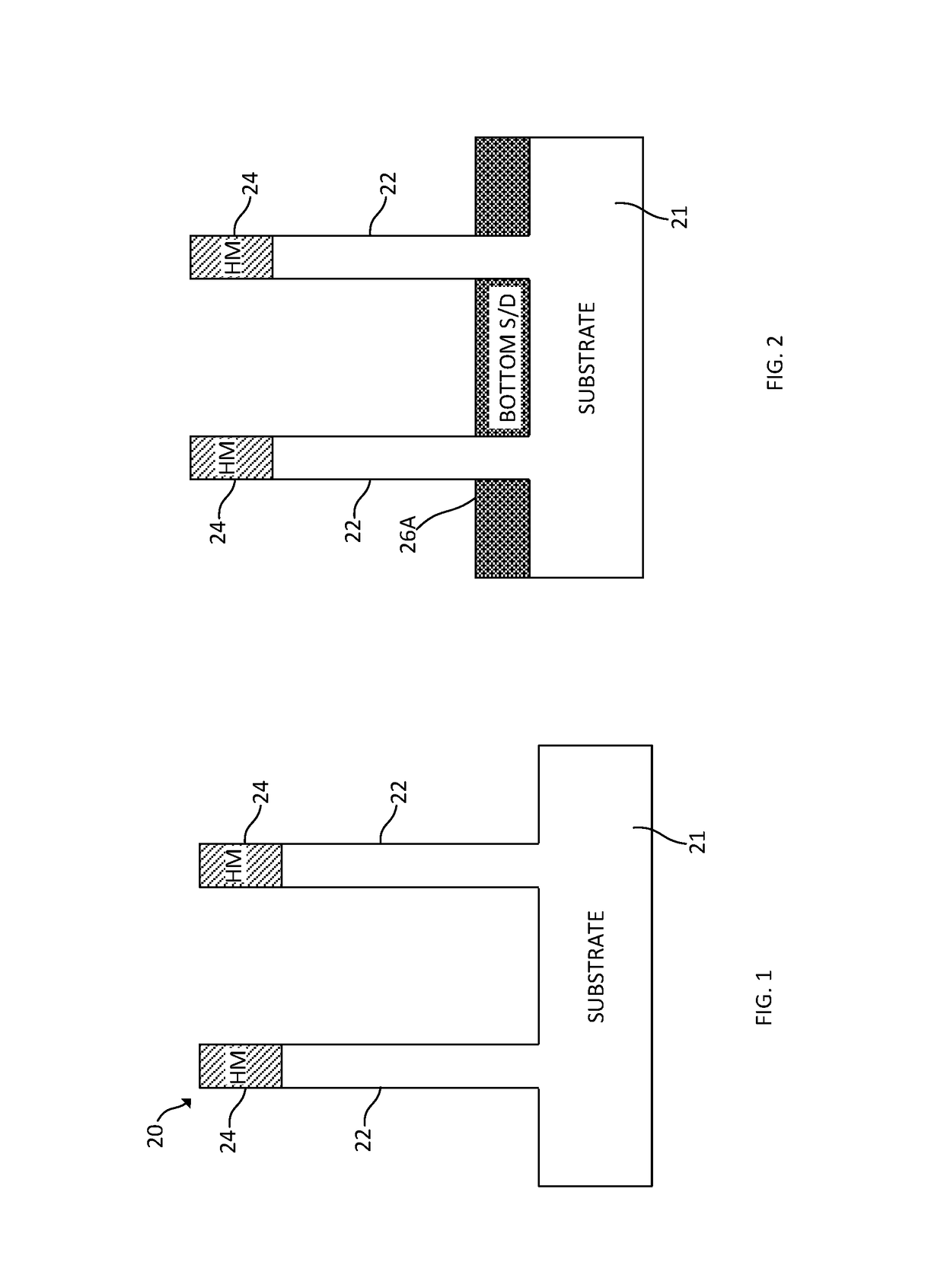
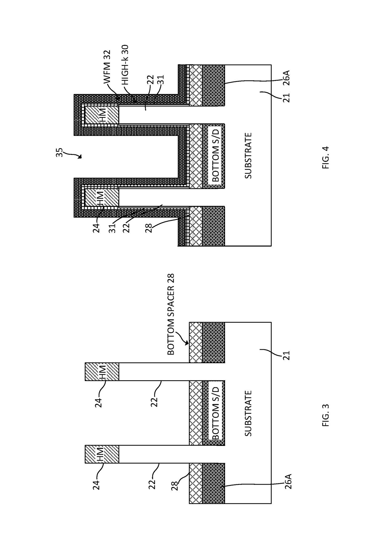
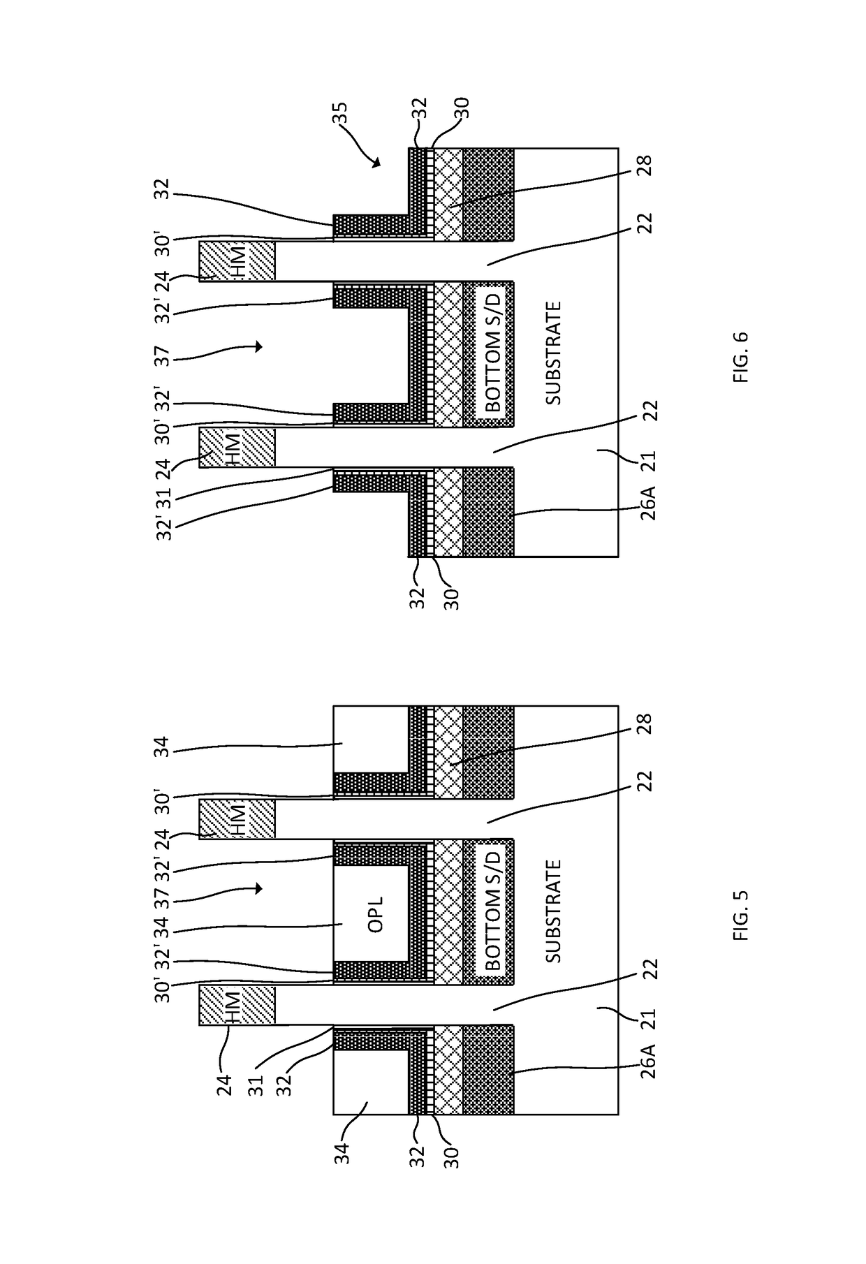
[0033]A structure 20 including a bulk semiconductor substrate 21 comprised of crystalline silicon is shown in FIG. 1. The substrate may be in the form of a wafer that is essentially undoped. An array of parallel fins 22 is formed from the substrate using, for example, a sidewall image transfer process. A hard mask (not shown) may be deposited over the substrate, including any features thereon, using conventional deposition techniques such as spin-on coating, CVD, plasma-assisted CVD, or other known techniques. The fins 22 are formed beneath portions of the hard mask...


PUM


Abstract

A vertical transport field-effect transistor includes a top source / drain region separated from an underlying gate stack by a multi-layer top spacer that includes an oxygen barrier layer beneath a top dielectric layer. Techniques for fabricating the transistor include depositing the oxygen barrier layer over the gate stack prior to depositing the top dielectric layer. The oxygen barrier layer blocks oxygen diffusion during deposition of the top dielectric layer, thereby avoiding damage to underlying interfacial and gate dielectric layers.

Description

BACKGROUND[0001]The present invention relates generally to the electrical, electronic and computer arts and, more particularly, to vertical transistor structures.[0002]Metal oxide semiconductor field-effect transistors (MOSFETs) include gate electrodes that are electrically insulated from operatively associated semiconductor channels by thin layers of dielectric material. MOSFETs having n-doped source and drain regions employ electrons as the primary current carriers while those having p-doped source and drain regions use holes as primary current carriers. Vertical transport field-effect transistors (VTFETs) have configurations wherein the current between the drain and source regions is substantially normal to the surface of the die. A vertical transport field-effect transistor may, for example, include a semiconductor pillar or fin having top and bottom regions comprising source / drain regions, the portion of the pillar between the source / drain regions defining a channel region. Jun...

Claims


Application Information

Patent Timeline
12 Mar 2019
Publication
US10229986B1
IPC
H01L29/66; H01L21/28; H01L29/78; H01L29/06
CPC
H01L29/6656; H01L29/0653; H01L29/7827; H01L21/28247; H01L29/66553; H01L29/6653; H01L29/66666; H01L29/513
Inventors
JAGANNATHAN, HEMANTH; LEE, CHOONGHYUN