Efficient spin-photon interface using glide-plane-symmetric waveguide

a waveguide and glide-plane technology, applied in the direction of electrical equipment, instruments, nanotechnology, etc., can solve the problem that the circularly polarized transition dipole moment emitter cannot efficiently couple to such waveguides, and achieve the effect of low loss and efficient coupling

Active Publication Date: 2019-04-16
UNIVERSITY OF COPENHAGEN
View PDF7 Cites 0 Cited by
  • Summary
  • Abstract
  • Description
  • Claims
  • Application Information

AI Technical Summary

Benefits of technology

[0016]The planar waveguide with glide-plane-symmetric nanostructures about a guiding region provides a waveguide, whose modes have electric fields with a strong in-plane circular polarisation. The modes of the structure can couple to the different spin states of quantum dots or any integrated quantum emitter, whose transition dipole moment is circularly polarised. Accordingly, the invention provides a photonic nanostructure that enables photon qubits to interact very efficiently with spin qubits, and thereby a device where a quantum emitter with a high efficiency can couple to the planar waveguide and be read out. It should be noted that “the circular polarized modes” are not circularly polarized in the conventional sense. In terms of the present invention and planar waveguides, the electric field vector is circularly polarized within the plane of the structure at the position of the emitter.
[0032]According to yet another advantageous embodiment, the planar waveguide comprises a second longitudinal region, where the first nanostructure and the second nanostructure are arranged mirror-symmetric about the guiding region of the waveguide. Thereby, the light propagating through the planar waveguide may couple efficiently to a conventional waveguide.
[0033]According to a particular advantageous embodiment, the planar waveguide comprises a transition region, advantageously arranged between the first longitudinal region and the second longitudinal region, and wherein the geometry of the first and the second nanostructure gradually changes from glide-plane symmetry to mirror symmetry. Thereby, the guided mode is gradually changed from a circular polarisation to a linear polarisation with low or no loss and may more efficiently be coupled to a conventional waveguide.
[0048]The planar waveguide is advantageously designed as a floating structure along at least a substantial part of the planar waveguide. Such a design minimises the losses by minimising light being coupled out of the plane.
[0058]This provides a planar waveguide, which is particularly suited for efficiently in-coupling photons emitted from a quantum emitter and out-coupling the photons to other optical devices.

Problems solved by technology

Therefore, the different spin states of quantum dots or any integrated quantum emitter with circularly polarized transition dipole moments cannot efficiently couple to such waveguides.

Method used


Image

  • Efficient spin-photon interface using glide-plane-symmetric waveguide
  • Efficient spin-photon interface using glide-plane-symmetric waveguide
  • Efficient spin-photon interface using glide-plane-symmetric waveguide

Examples


example 1

out and Single-Photon Diode

[0097]FIG. 7 illustrates a first optical device 101 implementing a planar waveguide 2 according to the invention, where FIG. 7c shows a Mach-Zehnder interferometer suggested for on-chip spin readout in the Heitler regime. The interaction with the quantum dot takes place in a section of the glide-plane-symmetric waveguide (GPW) 2 placed in path A. Path B includes a phase control, which is necessary to ensure that the interferometer is correctly balanced. FIG. 7a shows an external magnetic field, Bext, along the growth direction which splits the two circularly polarized transitions, denoted with dipoles σ+ and σ−. In addition to energetically splitting the two circular transitions, the external magnetic field suppresses the diagonal transitions denoted by the dashed arrows. FIG. 7b shows the phase and probability amplitude for a single photon forward-scattered in a GPW as a function of the directional β-factor. FIG. 7d shows the probabilities of a successful...

example 2

on-Demolition Measurement

[0102]Adding coherent control of the single electron spin qubit, allows us to create arbitrary superpositions of the two single electron ground-states, making additional applications attainable. Such control can be achieved both by optical methods and through in-plane oscillating magnetic fields, Bμw, created by a microwave source, which is shown schematically in FIG. 8a. Using this control a single-photon quantum non-demolition (QND) detector can be built by following methods known per se. Initialization of the spin qubit in the state |↑ can be done through optical spin pumping by driving the σ− transition. Next, a pi / 2-rotation of the spin qubit is carried out, making the transformations:

[0103]|↑〉⁢→π⁢ / ⁢2⁢12⁢(|↑〉+|↓〉),and⁢|↓〉⁢→π⁢ / ⁢2⁢12⁢(-|↑〉+|↓〉).

which can be done by Bμw. A single photon on resonance with the Bμw transition, |kb, will only obtain a phase shift when the quantum dot is in the state |↑. After the single photon has past the interaction region, ...

example 3

oton Transistor and cNot Gate

[0107]In Example 1 it was shown that using an MZI, the single-spin ground state of a trion can be efficiently read out, and in Example 2 it was illustrated how a single-photon can be used to control the internal state of the quantum dot.

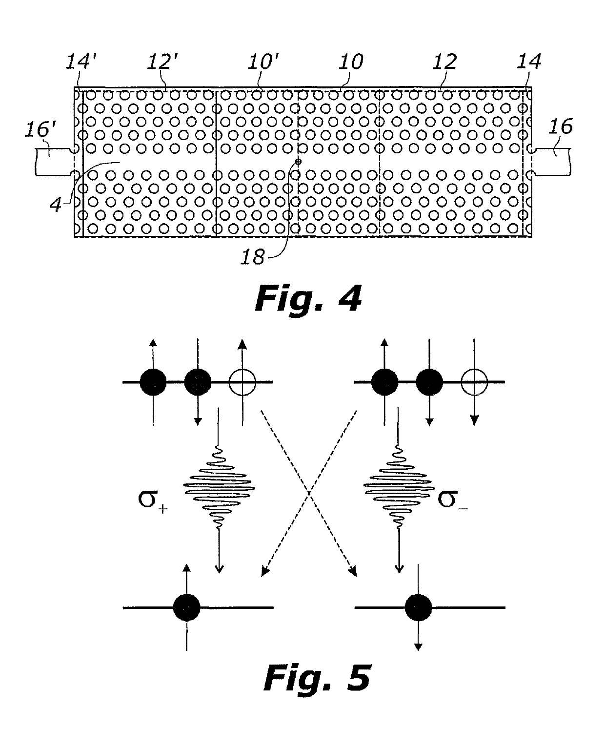
[0108]In this Example, we combine these two ideas into a single-photon transistor / switch, where a single gate photon controls the flow of subsequent photons. Again, a trion is used in an external magnetic field pointing along the growth direction. This is shown in FIG. 8a, where an external magnetic field, Bext, along the growth direction splits the two circularly polarized transitions, denoted with the dipoles moments σ+ and σ−. In addition to energetically splitting the two circular transitions the external magnetic field suppresses the diagonal transitions denoted by the dotted arrows. Coherent control of the spin qubit can be obtained through oscillating in-plane magnetic fields, generated by a microwave source on res...


PUM


Abstract

An optical device comprising a planar waveguide and a quantum emitter is presented. The planar waveguide comprises a longitudinal extending guiding region with a first side and a second side. A first nanostructure is arranged on the first side of the guiding region, and a second nanostructure is arranged on the second side of the guiding region. The planar waveguide includes a first longitudinal region where the first nanostructure and the second nanostructure are arranged substantially glide-plane symmetric about the guiding region of the planar waveguide, and the quantum emitter is coupled to the first longitudinal region of the planar waveguide.

Description

CROSS-REFERENCE TO RELATED APPLICATIONS[0001]This application is a § 371 national stage entry of International Application No. PCT / EP2015 / 063340, filed Jun. 15, 2015, which claims priority to European Patent Application No. 14172566.3 filed Jun. 16, 2014, the entire contents of which are incorporated herein by reference.FIELD OF THE INVENTION[0002]The present invention relates to an optical device comprising a planar waveguide and a quantum emitter.BACKGROUND OF THE INVENTION[0003]Data on everyday computers are comprised of bits, which are a binary sequence of zeroes and ones. These bits can be stored magnetically on hard drives or electrically on flash drives. In the last few decades quantum information processing using quantum bits or “qubits” has emerged as a completely new form of computation. Unlike a bit, a single qubit is a quantum mechanical object and can be in a combination or superposition of zero and one states. Qubits can be manipulated and processed to perform computat...

Claims


Application Information

Patent Timeline
Patent Type & Authority Patents(United States)
IPC IPC(8): G02B6/122B82Y20/00G02B1/00G02B6/12
CPCG02B6/1225B82Y20/00G02B6/1223G02B1/005G02F2202/32G02B2006/12078H01L25/00
Inventor MAHMOODIAN, SAHANDSÖLLNER, IMMO NATHANAELSTOBBE, SØRENLODAHL, PETER
Owner UNIVERSITY OF COPENHAGEN
Why Eureka
Try Eureka