Imaging device and electronic apparatus

a technology of electronic equipment and a camera, which is applied in the field of imaging devices, can solve the problems of high assembly accuracy, unmanufacturability of lenses, and increased number of lenses, and achieve the effects of high resolution, small size, and high pixel coun

Inactive Publication Date: 2019-06-25
SONY CORP
View PDF42 Cites 2 Cited by
  • Summary
  • Abstract
  • Description
  • Claims
  • Application Information

AI Technical Summary

Benefits of technology

[0015]According to the present technology, it is possible to make provision for a high pixel count and a wide angle with a small size and high resolution at low cost.

Problems solved by technology

However, when these problems are to be solved by only a lens system, the number of lenses is increased, and high assembly accuracy is required.
The problem of a need to make the lenses so small as to be unmanufacturable, for example, occurs.

Method used


Image

  • Imaging device and electronic apparatus
  • Imaging device and electronic apparatus
  • Imaging device and electronic apparatus

Examples


first embodiment

1. First Embodiment

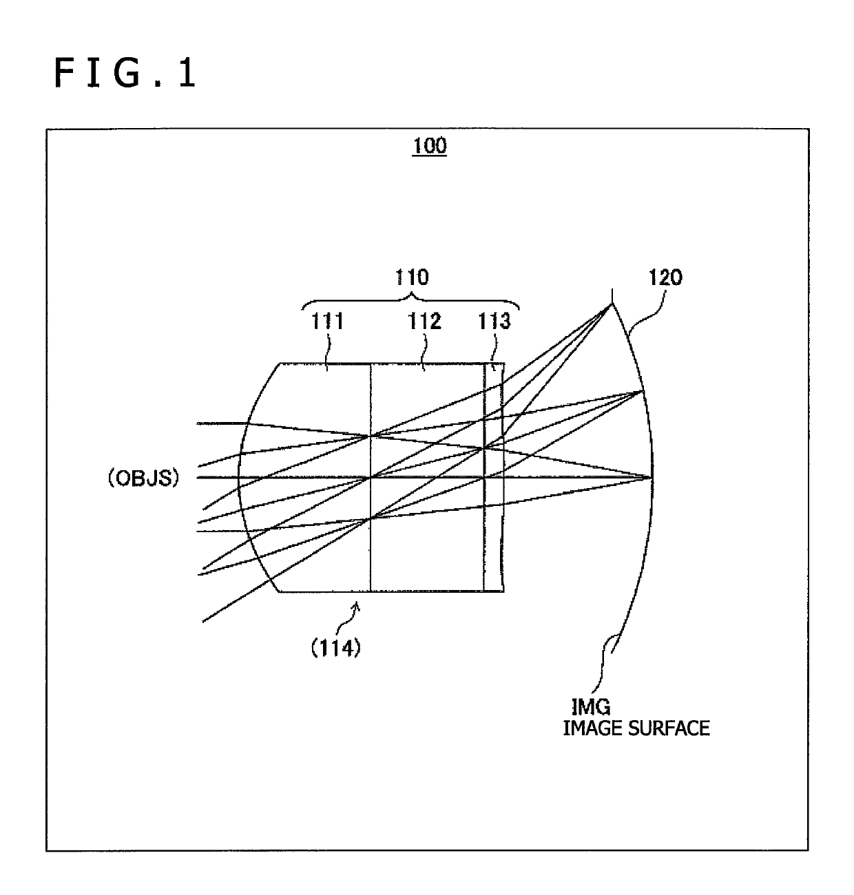
[0064]FIG. 1 is a diagram showing an example of configuration of an imaging device according to a present first embodiment.

[0065]As shown in FIG. 1, the imaging device 100 according to the present first embodiment includes a lens 110 and an imaging element 120 arranged in order from an object side OBJS to an image surface side.

[0066]This lens 110 is formed as a single focus lens.

[0067]The present imaging device 100 basically includes the imaging element 120 curved so as to have a concave surface facing the object side and one group of lenses 110.

[0068]The lenses 110 include a first lens 111 whose object side surface has a convex shape projecting to the object side, a glass substrate 112 as a transparent body provided with a diaphragm and an infrared cutoff filter, and a second lens 113, with the first lens 111, the glass substrate 112, and the second lens 113 arranged in order from the object side to the image surface side without an air being interposed therebetw...

first example

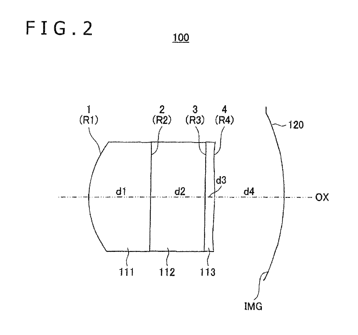
[0107]The numerical values of the first example are shown in Table 1, Table 2, Table 3, and Table 4. The numerical values of the first example correspond to the lens 110 of FIG. 1.

[0108]The first example is a design example for a 3-megapixel (Mega pixel) CMOS imager having a ⅙ size and a 1.1-μm pitch.

[0109]As described above, the present first example includes the imaging element 120 curved so as to have a concave surface facing the object side and one group of lenses 110.

[0110]The lenses 110 include the first lens 111 whose object side surface has a convex shape projecting to the object side, the glass substrate 112 provided with a diaphragm and an infrared cutoff filter, and the second lens 113, with the first lens 111, the glass substrate 112, and the second lens 113 arranged in order from the object side to the image surface side without an air being interposed therebetween.

[0111]The first lens 111 is desirably realized by providing an ultraviolet (UV) curing replica lens on the...

second embodiment

2. Second Embodiment

[0130]FIG. 5 is a diagram showing an example of configuration of an imaging device according to a present second embodiment.

[0131]The imaging device 100A according to the second embodiment shown in FIG. 5 and the imaging device 100 according to the first embodiment shown in FIG. 1 are different from each other in the following respect.

[0132]In the imaging device 100A, a first lens 111A is formed by a first lens element 1111 and a second lens element 1112, and a glass substrate 112A is formed by a first glass substrate 1121 and a second glass substrate 1122. In the second embodiment, the first lens 111A is formed on the first glass substrate 1121, and a second lens 113A is formed on the second glass substrate 1122.

[0133]FIG. 6 is a diagram showing surface numbers given to the lenses and the substrate of the imaging device according to the present second embodiment.

[0134]Specifically, a surface number of number one is given to the object side surface (convex surfac...


PUM


Abstract

An electronic apparatus includes an imaging device and a signal processing circuit for performing signal processing on an output signal of the imaging device. The imaging device includes one group of lenses, and an imaging element on which an image is formed through the lenses, and the lenses include a first lens having an object side surface in a convex shape projecting to an object side, a transparent body, and a second lens, the first lens, the transparent body, and the second lens being arranged in order from the object side to an image surface side without an air being interposed between the first lens, the transparent body, and the second lens, and the imaging element is curved so as to have a concave surface facing the object side.

Description

TECHNICAL FIELD[0001]The present technology relates to an imaging device applied to an imaging apparatus and an electronic apparatus.BACKGROUND ART[0002]High resolution, low cost, and miniaturization have been strongly demanded for imaging apparatuses mounted in mobile telephones, personal computers (PC), and the like in recent years.[0003]The cell pitches of imaging elements such as CCD (Charge Coupled Device) and CMOS (Complementary Metal Oxide Semiconductor) image sensors and the like have been dramatically decreased, and optical systems are required to have high image forming performance that suppresses optical aberrations, particularly axial chromatic aberration more than ordinary optical systems.[0004]However, when these problems are to be solved by only a lens system, the number of lenses is increased, and high assembly accuracy is required.[0005]The problem of a need to make the lenses so small as to be unmanufacturable, for example, occurs.[0006]One method for solving these...

Claims


Application Information

Patent Timeline
Patent Type & Authority Patents(United States)
IPC IPC(8): G02B27/14G02B13/00H04N5/369H04N5/357G02B13/14
CPCG02B13/001G02B13/003H04N5/3696G02B13/14H04N5/3572G02B13/0035H04N25/615
Inventor BABA, TOMOHIKO
Owner SONY CORP
Why Eureka
Try Eureka