
Light emitting diode having light blocking layer

a light blocking layer and light emitting diode technology, applied in the direction of basic electric elements, electrical appliances, semiconductor devices, etc., can solve the problems of reducing light output under the same current density conditions, light emitting diode chips suffer from resins are vulnerable to heat, etc., to achieve small light emitting surface and high output performance without deterioration in luminous efficacy

Active Publication Date: 2019-07-02
SEOUL VIOSYS CO LTD
View PDF16 Cites 0 Cited by
  • Summary
  • Abstract
  • Description
  • Claims
  • Application Information

AI Technical Summary

Benefits of technology

[0007]Exemplary embodiments of the invention may provide a light emitting diode that has a small light emitting surface and exhibits high output performance without deterioration in luminous efficacy.
[0008]Exemplary embodiments may provide a technique that can easily adjust the size of the light emitting surface of the light emitting diode while maintaining high output performance of the light emitting diode.

Problems solved by technology

However, size reduction of a light emitting diode chip generally results in a reduction of light output under the same current density conditions.
However, light emitting diode chips suffer from deterioration in luminous efficacy due to a “drooping” phenomenon at high current density, as is well known in the art.
Although the phosphors are generally mixed with a transparent resin, such as a silicone resin or an epoxy resin, such resins are vulnerable to heat.
In addition, although two or more kinds of phosphors may be used in order to improve color rendering and color reproduction properties, it is difficult to achieve uniform mixing of these phosphors.
As a result, color deviation is likely to occur between light emitting is diodes to which the phosphors are applied.
Moreover, light subjected to wavelength conversion by one kind of phosphor can be absorbed or interfered with by another kind of phosphor, thereby providing low efficiency in wavelength conversion and making it difficult to improve the color rendering properties.

Method used


Image

  • Light emitting diode having light blocking layer
  • Light emitting diode having light blocking layer
  • Light emitting diode having light blocking layer

Examples


Embodiment Construction

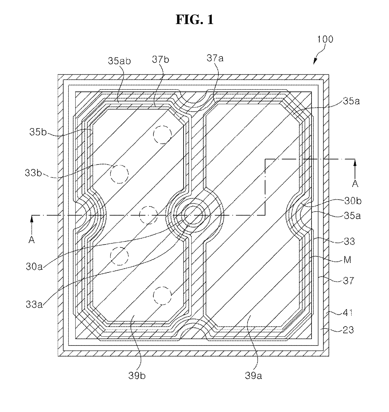
[0033]Hereinafter, exemplary embodiments of the invention will be described in detail with reference to the accompanying drawings. The following embodiments are provided by way of example so as to fully convey the inventive concepts to those skilled in the art to which the present disclosure pertains. Accordingly, the inventive concepts are not limited to the embodiments disclosed herein and can also be implemented in different forms. In the drawings, widths, lengths, thicknesses, and the like of elements can be exaggerated for clarity and descriptive purposes. When an element is referred to as being “disposed above” or “disposed on” another element, it can be directly “disposed above” or “disposed on” the other element, or intervening elements can be present. Throughout the specification, like reference numerals denote like elements having the same or similar functions.

[0034]In accordance with an exemplary embodiment, a light emitting diode includes: a substrate that includes an up...


PUM


Abstract

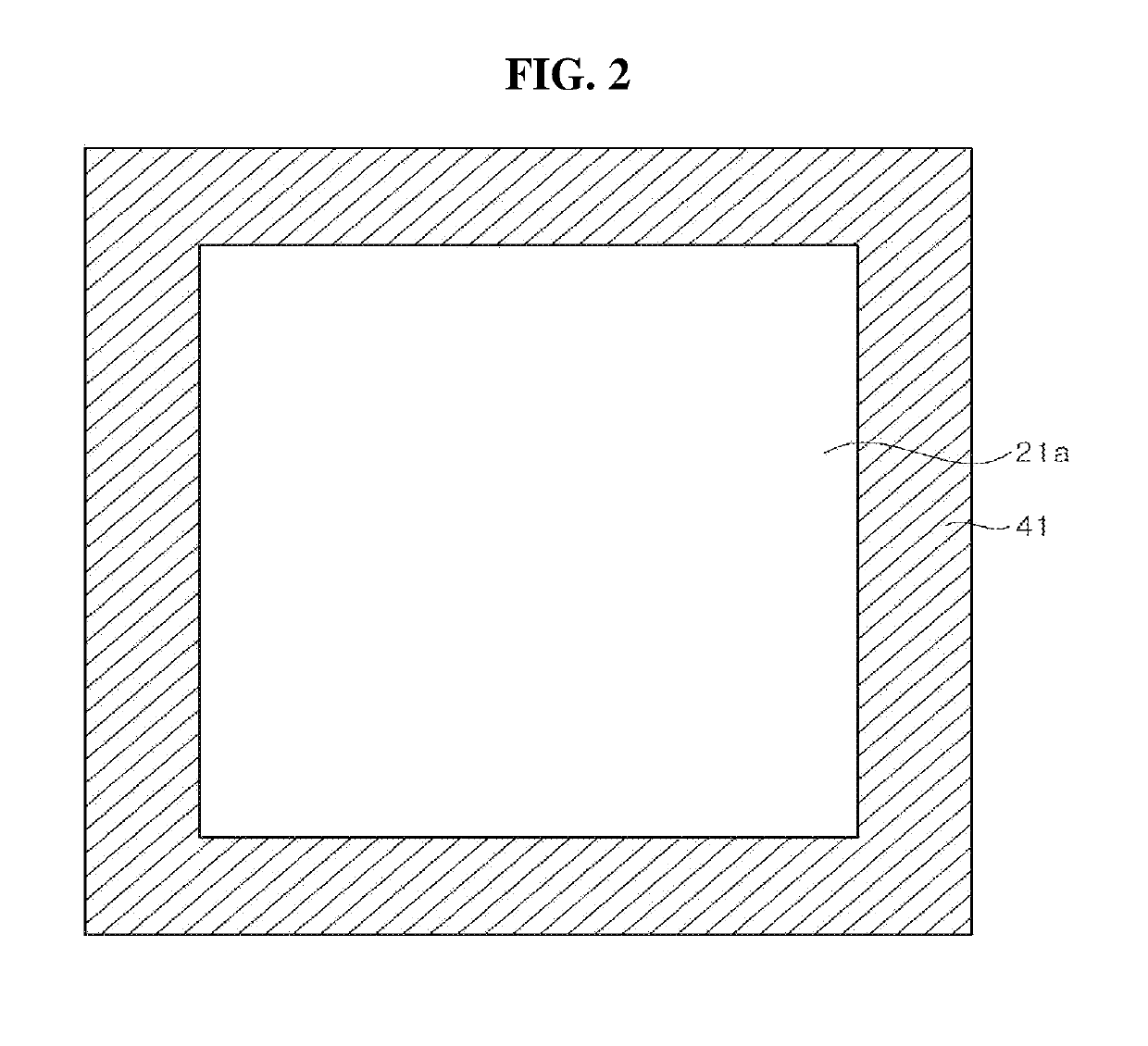
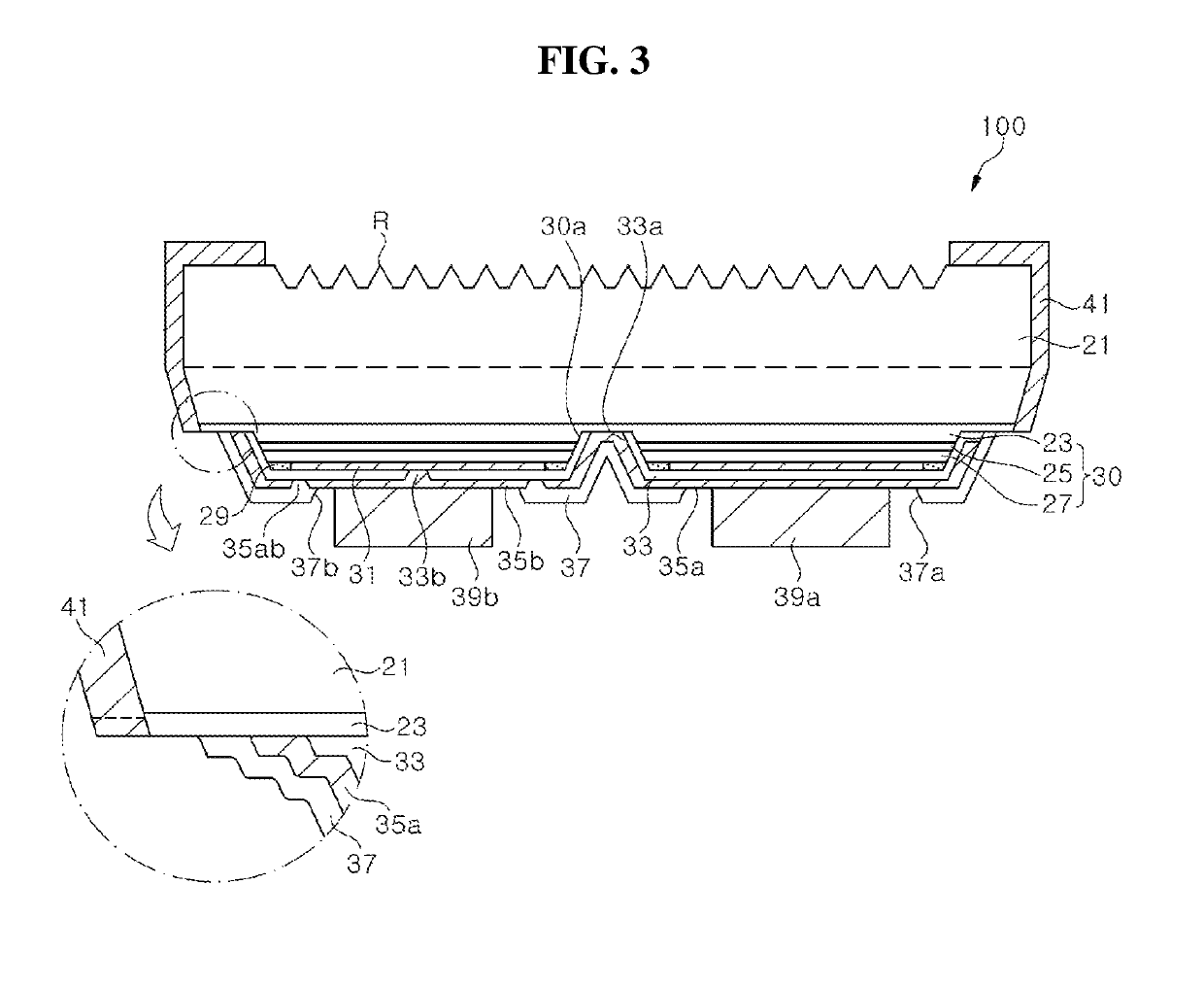
A light emitting diode including a light blocking layer is disclosed. The light emitting diode includes: a substrate including an upper surface and side surfaces; a semiconductor stack disposed under the substrate and including a first conductivity type semiconductor layer, a second conductivity type semiconductor layer, and an active layer interposed between the first conductivity type semiconductor layer and the second conductivity type semiconductor layer; and a light blocking layer covering the upper surface and the side surfaces of the substrate to define a light emitting surface on the upper surface of the substrate. The size of a light emitting surface of the light emitting diode can be easily controlled using the light blocking layer.

Description

CROSS-REFERENCE TO RELATED APPLICATION[0001]This application claims priority to and the benefit of Korean Patent Application No. 10-2016-0158391, filed on Nov. 25, 2016, and Korean Patent Application No. 10-2017-0024857, filed on Feb. 24, 2017, which are all incorporated by reference for all purposes as if fully set forth herein.BACKGROUNDField[0002]Exemplary embodiments relate to a light emitting diode. More particularly, exemplary embodiments relate to a light emitting diode including a light blocking layer.Discussion of Background[0003]Recently, group III-based nitrides, such as gallium nitride (GaN) and aluminum nitride (AlN) have been used as materials for light sources in the visible range and the ultraviolet range. In particular, blue and green light emitting diodes using indium gallium nitride (InGaN) are used in various applications, such as large natural color flat displays, signal lamps, interior lighting, high density light sources, camera flashes, high resolution output...

Claims


Application Information

Patent Timeline
Patent Type & Authority Patents(United States)
IPC IPC(8): H01L33/00H01L33/46H01L33/62H01L33/24H01L33/22H01L33/10H01L33/44H01L33/38H01L33/20
CPCH01L33/46H01L33/10H01L33/22H01L33/24H01L33/62H01L2933/0033H01L33/20H01L33/382H01L33/44H01L2933/0025H01L33/504H01L33/505H01L2933/0041H01L2933/0066
Inventor JANG, JONG MINKIM, CHANG YEONLIM, JAE HEE
Owner SEOUL VIOSYS CO LTD
Learn More