
Voltage-tunable wavelength-agile 2D material-based light-emitting transistors

a technology of light-emitting transistors and wavelength-agile materials, which is applied in the field of voltage-tunable wavelength-agile 2d material-based light-emitting transistors, can solve the problems that the voltage-tunable wavelength-agile photon emission from these 2d materials at room temperature currently does not exist, and can not be reliably used for military purposes. , to achieve the effect of low cos

Active Publication Date: 2019-08-13
THE UNITED STATES OF AMERICA AS REPRESENTED BY THE SECRETARY OF THE NAVY
View PDF5 Cites 7 Cited by
  • Summary
  • Abstract
  • Description
  • Claims
  • Application Information

AI Technical Summary

Benefits of technology

The patent is about a technology called 2D LET that can be used to enhance the abilities of soldiers and drones in the military. This technology is affordable, flexible, and can be worn like a suit or used as a contact lens. It can help improve information warfare, provide better situational awareness, and help ensure that the military has the best technology to communicate and monitor their activities. Overall, 2D LET can make the Naval Force more effective and efficient.

Problems solved by technology

However, conventional optoelectric emitters and optoelectric detectors based on 3D bulk semiconductors are not tunable with sufficient precision to be reliably used for some military purposes.
However, scalable, CMOS-compatible, voltage-tunable wavelength-agile photon emission from these 2D materials at room temperature currently does not exist.

Method used


Image

  • Voltage-tunable wavelength-agile 2D material-based light-emitting transistors
  • Voltage-tunable wavelength-agile 2D material-based light-emitting transistors
  • Voltage-tunable wavelength-agile 2D material-based light-emitting transistors

Examples


Embodiment Construction

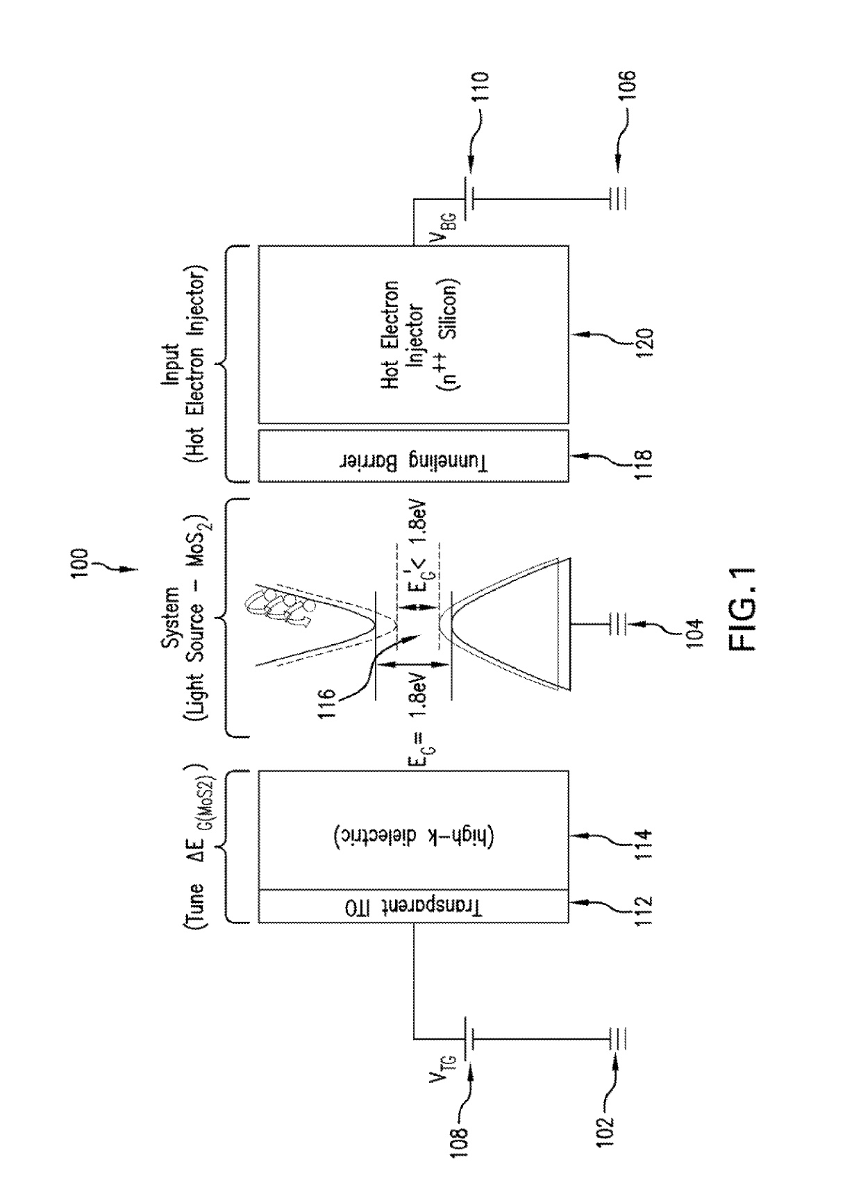
[0019]Aspects of the present invention are drawn to a system and method for using a 2D material and ion gel top gate electric to enable voltage controlled wavelength agile light emission.

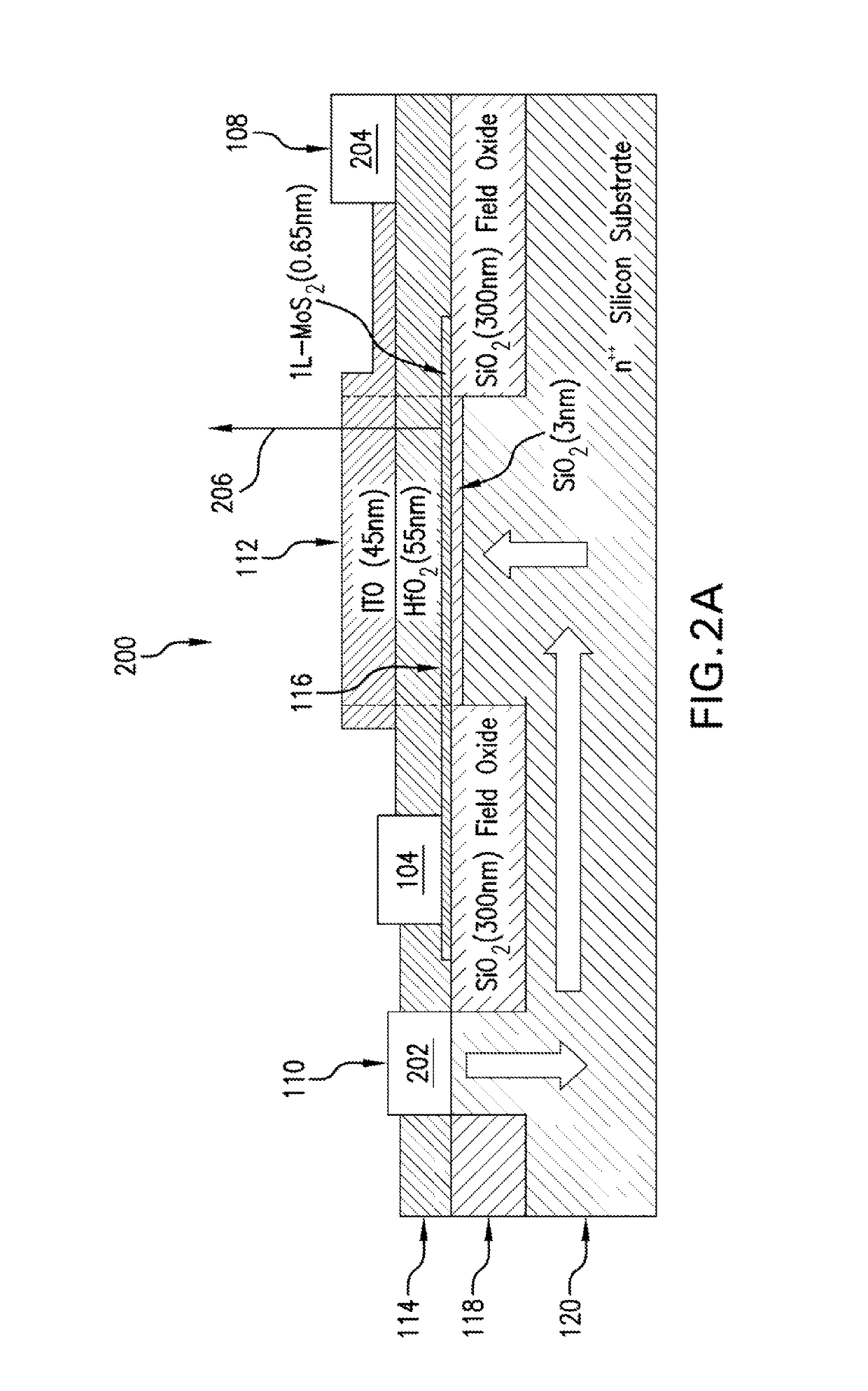
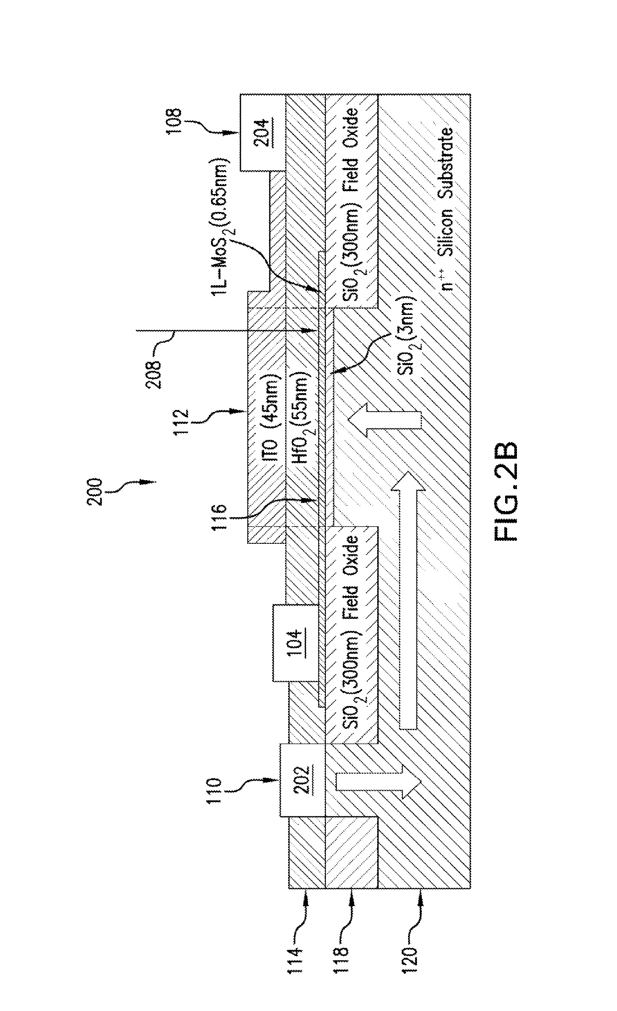
[0020]In accordance with a first aspect of the present invention a highly doped substrate, which serves as the hot electron emitter, is provided along with a tunneling barrier stacked on top of the substrate, and a 2D semiconductor material stacked on top of the tunneling barrier. Next, a top gate dielectric material is stacked on top of the semiconductor material and finally a collector layer is disposed on top.

[0021]An emitter-base voltage (VEB), or similarly a back-gate voltage (VBG), is applied to the highly doped substrate such that hot electrons quantum mechanically tunnel from the highly doped substrate, through the tunneling barrier and into the conduction band of the 2D semiconductor material.

[0022]As the hot electrons relax within the conduction band of the 2D material, they eventually rec...


PUM


Abstract

An optoelectronic device is provided that includes a doped substrate, a tunneling barrier, a direct bandgap two dimensional semiconductor material, a hot electron emitter, a gate electrode, and a voltage bias. The hot electron emitter injects hot electrons from the underlying substrate into the conduction band of the direct bandgap two dimensional semiconductor material via quantum tunneling. The gate electrode is operable to provide the voltage bias in a direction normal to the X-Y plane of the direct bandgap two dimensional semiconductor material so as to generate an electric field perpendicular to the direct bandgap two dimensional semiconductor material. The voltage bias provided by the gate is operable to change an optical bandgap of the direct bandgap two dimensional semiconductor material continuously from the visible to the mid-infrared spectral regime via an electric dipole layer enhanced Giant Stark Effect for electrically-tunable hot electron luminescence applications.

Description

FEDERALLY-SPONSORED RESEARCH AND DEVELOPMENT[0001]The United States Government has ownership rights in this invention. Licensing inquiries may be directed to Office of Research and Technical Applications, Space and Naval Warfare Systems Center, Pacific, Code 72120, San Diego, Calif., 92152; telephone (619) 553-5118; email: ssc_pac_t2@navy.mil. Reference Navy Case No. 106,251.BACKGROUND OF THE INVENTION[0002]The present invention is generally drawn to optoelectric emitters and optoelectric detectors. Optoelectric emitters and optoelectric detectors are used for many purposes, including communications (e.g. optical interconnects, on-chip integrated photonic components) in both the civilian world and the military world. Some optoelectric emitters and optoelectric detectors have a small spectrum of operation, whereas others have a relatively broad spectrum of operation. Further, some are tunable over a spectral range. However, conventional optoelectric emitters and optoelectric detector...

Claims


Application Information

Patent Timeline
IPC IPC(8): H01L33/00H05B33/08H01L33/34H01L31/112H01L33/26H01L31/032H05B44/00
CPCH01L33/0041H01L31/112H01L31/032H01L33/26H01L33/04H01L33/42
Inventor TORRES, JR., CARLOS M.ADLEMAN, JAMES R.LU, RYAN P.RAMIREZ, AYAX D.
Owner THE UNITED STATES OF AMERICA AS REPRESENTED BY THE SECRETARY OF THE NAVY
Learn More