Shift register, display device provided with same, and method for driving shift register

a shift register and display device technology, applied in the field of active matrix display devices, can solve the problems of abnormal operation, fluctuation of the voltage of scanning signal gout, and inability to simultaneously transmit image signals representing pixel voltages, so as to reduce the scale of the overall shift register circuit, and reduce the thickness of the bezel in the display device

Active Publication Date: 2019-11-12
SHARP KK
View PDF13 Cites 6 Cited by
  • Summary
  • Abstract
  • Description
  • Claims
  • Application Information

AI Technical Summary

Benefits of technology

[0087]In the first aspect of the present invention, the stabilization node that contributes to stabilizing the output control node and the stabilization node controller that controls the level (voltage) of the stabilization node are provided in each stage circuit group that includes two or more adjacent stages (stage circuits) of the shift register. In other words, the stabilization control node and the stabilization node controller are shared by multiple stage circuits. This reduces the scale of the overall shift register circuit. Therefore, the area occupied by the shift register in the corresponding region on one of the substrates of the display device can be reduced. This, in turn, makes it possible to reduce the thickness of the bezels in a display device.
[0088]In the second aspect of the present invention, the switching elements of the stabilization node controller (that is, the stabilization node OFF-switching element and the stabilization node ON-switching element) are shared by multiple stage circuits. Therefore, the stabilization node controller requires fewer switching elements per shift register stage than in conventional configurations. Applying this shift register to a monolithic gate driver for driving the scanning signal lines of a display device makes it possible to provide a monolithic gate driver that includes fewer elements than in conventional configurations. This, in turn, makes it possible to reduce the thickness of the bezels in a display device.
[0089]In the third aspect of the present invention, the load applied to the output control node is divided evenly among the stage circuits of the P stages (where P is an integer greater than or equal to 2) included in the stage circuit group. This makes it possible to further stabilize the operation of the shift register.
[0090]In the fourth aspect of the present invention, the stabilization node controller does not include any switching elements to which clock signals are input. Therefore, each stage circuit includes fewer switching elements to which a clock signal is input than in conventional configurations. This reduces the clock load in comparison with conventional configurations. This, in turn, reduces power consumption in comparison with conventional configurations.
[0091]The fifth aspect of the present invention makes it possible to provide a monolithic gate driver that does not have a vertical inversion feature (that is, a feature for switching the order in which the scanning signal lines are scanned) using fewer elements than in a conventional configuration.
[0092]The sixth aspect of the present invention makes it possible to implement a vertical inversion feature simply by including two switching elements (that is, the first output control node ON / OFF-switching element and the second output control node ON / OFF-switching element) on the input side of the output control node in each stage circuit and then controlling the levels of the first scanning order instruction signal and the second scanning order instruction signal. In other words, the number of switching elements required to implement a vertical inversion feature is less than in conventional configurations. Moreover, similar to in the second aspect of the present invention, the stabilization node controller requires fewer switching elements per shift register stage than in conventional configurations. This makes it possible to provide a monolithic gate driver that has a vertical inversion feature using significantly fewer elements than in a conventional configuration.

Problems solved by technology

However, the source bus lines cannot simultaneously transmit several rows worth of the image signals that represent pixel voltages.
However, in the configuration described above, any noise that occurs due to the clock signal (that is, due to the first gate clock signal CKA) during the normal operation period can potentially cause fluctuations in the voltage of the scanning signal GOUT, which is supposed to be fixed at the low level during this period.
This can potentially cause abnormal operation and increased power consumption.

Method used


Image

  • Shift register, display device provided with same, and method for driving shift register
  • Shift register, display device provided with same, and method for driving shift register
  • Shift register, display device provided with same, and method for driving shift register

Examples


embodiment 1

[0147]

[0148]

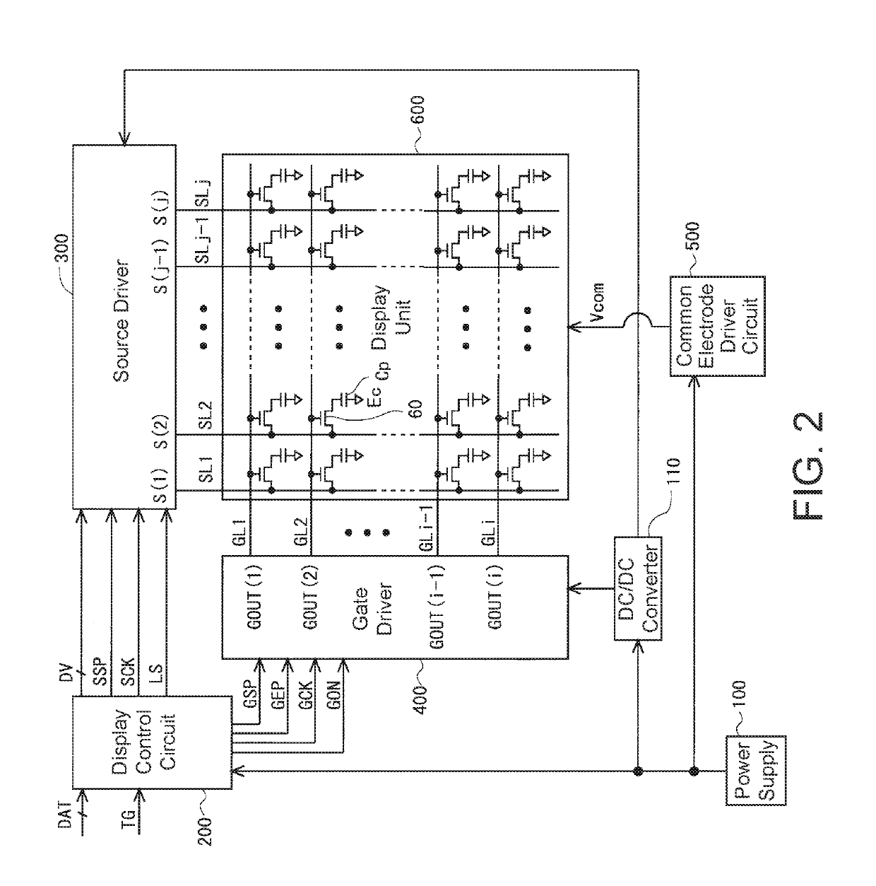
[0149]FIG. 2 is a block diagram illustrating an overall configuration of an active-matrix liquid crystal display device according to Embodiment 1 of the present invention. As illustrated in FIG. 2, this liquid crystal display device includes a power supply 100, a DC / DC converter 110, a display control circuit 200, a source driver (an image signal line driver circuit) 300, a gate driver (a scanning signal line driver circuit) 400, a common electrode driver circuit 500, and a display unit 600. In the present embodiment, the gate driver 400 and the display unit are formed on the same substrate (here, on a TFT substrate that is one of the two substrates included in a liquid crystal panel). In other words, the gate driver 400 of the present embodiment is a monolithic gate driver.

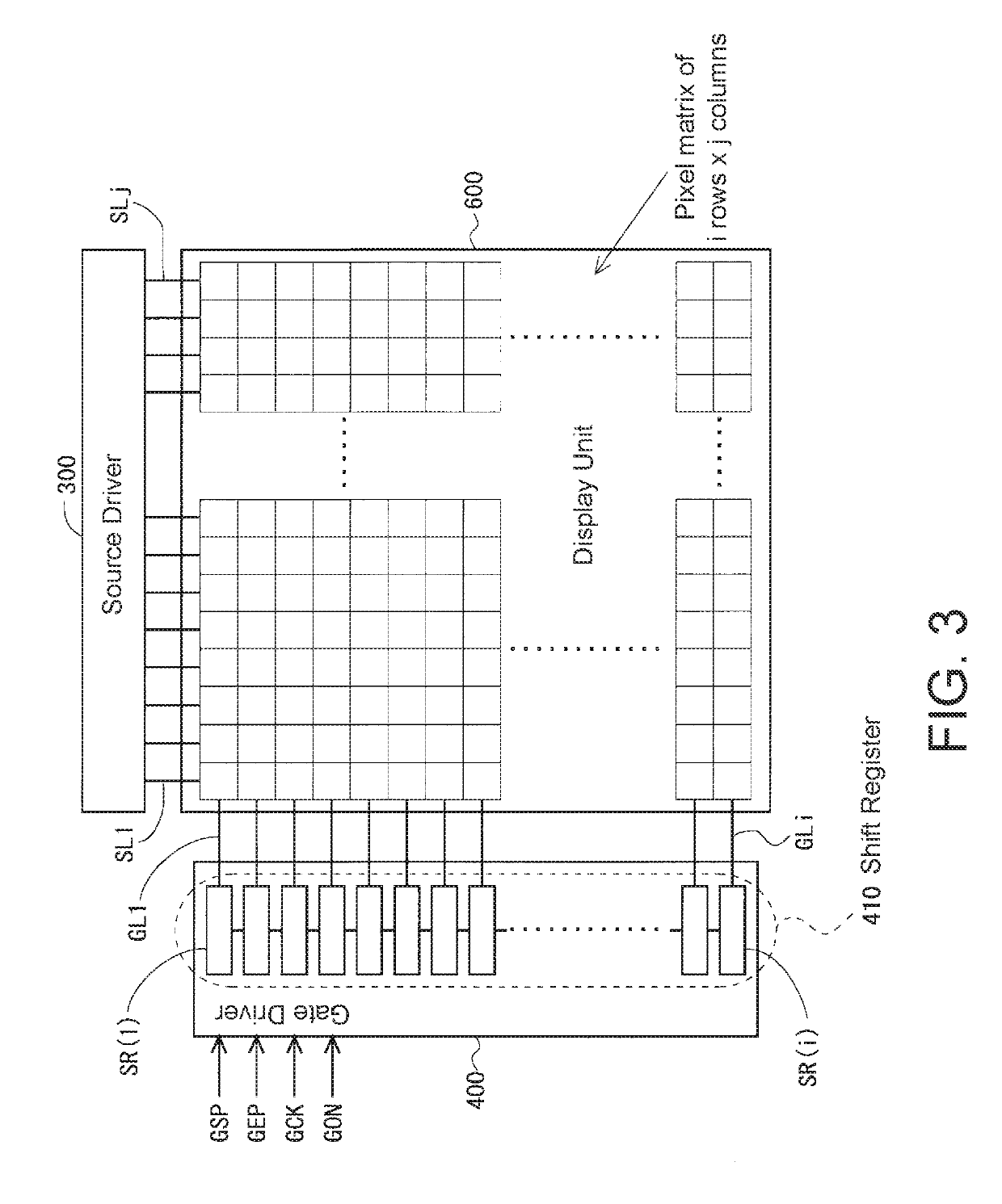
[0150]The display unit 600 includes a plurality of (j) source bus lines (image signal lines) SL1 to SLj, a plurality of (i) gate bus lines (scanning signal lines) GL1 to GLi, and a plurality of (i×j) ...

embodiment 2

[0224]

[0225]Next, Embodiment 2 of the present invention will be described. In the present embodiment, a gate driver 400 is a monolithic gate driver that has a vertical inversion feature (a feature for switching the order in which the gate bus lines are scanned). To implement this vertical inversion feature, in the present embodiment, a first scanning order instruction signal UD1 and a second scanning order instruction signal UD2 are input to the gate driver 400 from a display control circuit 200 in addition to a gate start pulse signal GSP, a gate end pulse signal GEP, gate clock signals GCK, and a stabilization control signal GON. Note that in the present specification, scanning the gate bus lines in the “first row, second row, . . . , (i−1)th row, ith row” order will be referred to as “forward scanning,” while scanning the gate bus lines in the “ith row, (i−1)th row, . . . , second row, first row” order will be referred to as “reverse scanning.”

[0226]

[0227]FIG. 23 is a block diagr...

embodiment 3

[0278]

[0279]Next, Embodiment 3 of the present invention will be described. Similar to in Embodiment 2 as described above, in the present embodiment a gate driver 400 is a monolithic gate drivers that has a vertical inversion feature. Unlike Embodiment 2, however, the present embodiment utilizes a configuration in which the first scanning order instruction signal UD1 and the second scanning order instruction signal UD2 are not used.

[0280]

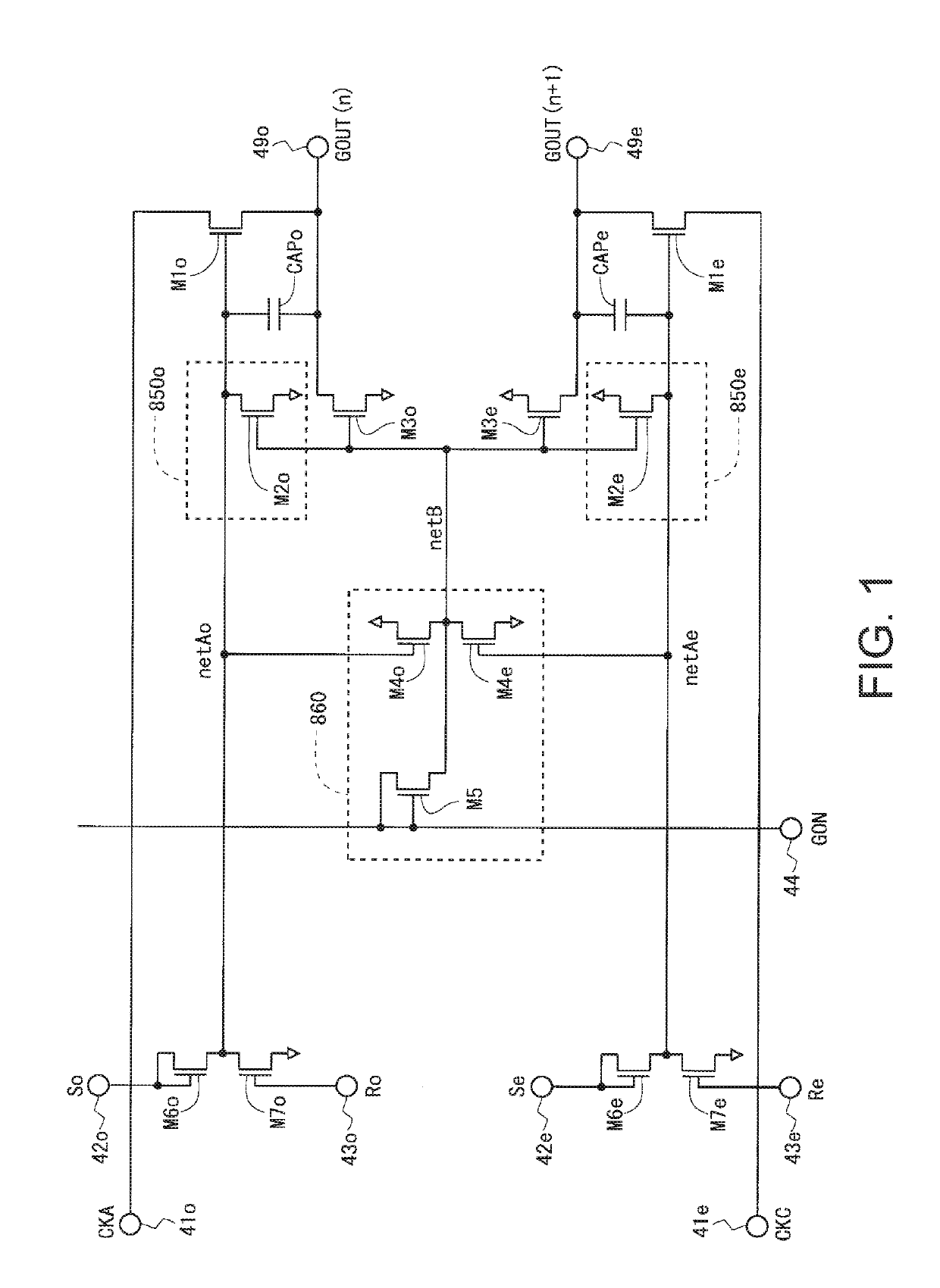
[0281]FIG. 31 is a block diagram illustrating a configuration of a shift register 410 in the gate driver 400 in Embodiment 3 of the present invention. Similar to in Embodiment 1, in the present embodiment, two adjacent stage circuits SR are treated as one stage circuit group SRG. The stage circuit SR of each odd-numbered stage includes an input terminal for receiving one of the gate clock signals GCK, an input terminal for receiving a low-level DC supply voltage VSS, an input terminal for receiving a set signal S1o, an input terminal for receiving a ...


PUM

PropertyMeasurementUnit
OFF-level supply voltageaaaaaaaaaa
voltageaaaaaaaaaa
pixel voltagesaaaaaaaaaa

Abstract

The present invention provides a monolithic gate driver that includes fewer elements than in conventional configurations. In one aspect, a plurality of stages included in a shift register are divided into a plurality of stage circuit groups, where each stage circuit group includes the stage circuits of P adjacent stages (two stages, for example). Each stage circuit group includes a stabilization node and a stabilization node controller that controls the voltage of the stabilization node. The stabilization node controller includes: thin-film transistors in which the gate terminals thereof are connected to output control nodes, the drain terminals thereof are connected to the stabilization node, and the source terminals thereof are connected to an input terminal for a DC supply voltage; and a thin-film transistor for changing the voltage of the stabilization node to a high level.

Description

TECHNICAL FIELD[0001]The present invention relates to an active-matrix display device, and more particularly to a shift register in a scanning signal line driver circuit for driving scanning signal lines in a display unit of an active-matrix display device.BACKGROUND ART[0002]Active-matrix liquid crystal display devices that include a plurality of source bus lines (image signal lines) and a plurality of gate bus lines (scanning signal lines) are a conventionally well-known technology. In past implementations of this type of liquid crystal display device, a gate driver (scanning signal line driver circuit) for driving the gate bus lines was often packaged as an integrated circuit (IC) chip that was then mounted on the periphery of a substrate included in the liquid crystal panel. In recent years, however, it has gradually become more common to form the gate driver directly on a TFT substrate, which is one of the two glass substrates included in the liquid crystal panel. Such gate dri...

Claims


Application Information

Patent Timeline
Patent Type & Authority Patents(United States)
IPC IPC(8): G11C19/00G09G3/20G09G3/36G11C19/28G02F1/133G11C8/04
CPCG02F1/133G09G3/3688G11C19/28G09G3/2011G11C8/04G09G3/3677G09G2300/0408G09G2310/0286G09G2310/0248G09G2330/021
Inventor IWASE, YASUAKIWATANABE, TAKUYA
Owner SHARP KK
Why Eureka
Try Eureka