Supercharge Your Innovation With Domain-Expert AI Agents!

Optoelectronic semiconductor chip and method for manufacturing an optoelectronic semiconductor chip

a technology of optoelectronic semiconductor and semiconductor chip, which is applied in the direction of diodes, semiconductor devices, radio frequency controlled devices, etc., can solve the negative effect of semiconductor chip optical properties, and achieve the effect of reducing the loss of absorption, which occurs particularly at the contact structure of the semiconductor chip

Active Publication Date: 2019-11-12
OSRAM OLED
View PDF22 Cites 0 Cited by
  • Summary
  • Abstract
  • Description
  • Claims
  • Application Information

AI Technical Summary

Benefits of technology

This patent describes an optoelectronic semiconductor chip that reduces absorption losses compared to conventional chips. The chip has a conductive layer, a filter layer, and a contact layer, all arranged on the main surface. The flat surface makes it easy to form the layers. The filter layer protects the chip in the active area. In one embodiment, the filter layer is located between the second contact element and the second semiconductor area to reduce radiation losses. Overall, this design improves the efficiency and performance of optoelectronic semiconductor chips.

Problems solved by technology

If this contact layer is relatively thick and thus enables good electrical conductivity on one hand, it also has a negative effect on the optical properties of the semiconductor chip on the other hand, since radiation is absorbed more strongly in a thicker contact layer.

Method used


Image

  • Optoelectronic semiconductor chip and method for manufacturing an optoelectronic semiconductor chip
  • Optoelectronic semiconductor chip and method for manufacturing an optoelectronic semiconductor chip
  • Optoelectronic semiconductor chip and method for manufacturing an optoelectronic semiconductor chip

Examples


Embodiment Construction

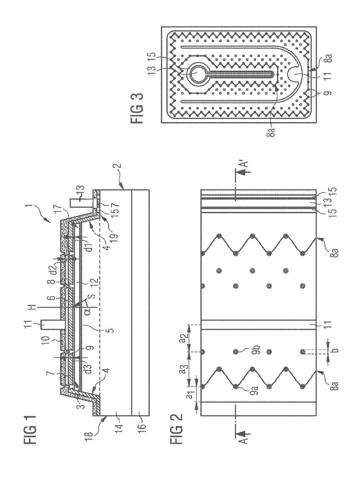
[0046]FIG. 1 shows a section of a schematic cross-sectional view of an embodiment of an optoelectronic semiconductor chip 1 described here. The semiconductor chip 1 comprises a semiconductor body 2 with a main surface 3 and several side surfaces 4 arranged transversely to the main surface 3, in particular at an angle greater than 90°. Furthermore, semiconductor body 2 has an active zone 5, which is intended for the generation of electromagnetic radiation S. During operation, some of the generated radiation S passes through the main surface 3 of the semiconductor body 2.

[0047]In this embodiment, the semiconductor body 2 has a mesa-shaped region 17, which is bounded at the top by the main surface 3 and at the periphery by oblique side surfaces. Furthermore, the semiconductor body 2 has a rectangular region 18, on which the mesa-shaped region 17 is arranged. The mesa-shaped region 17 is protruded laterally, i.e., in a direction essentially parallel to the main surface 3, at least in so...


PUM


Abstract

An optoelectronic semiconductor chip and a method for manufacturing an optoelectronic semiconductor chip are disclosed. In an embodiment the semiconductor chip includes a semiconductor body having a main surface and at least one side surface arranged transversely to the main surface, a contact layer arranged on the main surface of the semiconductor body and containing an electrically conductive material, a filter layer arranged on the contact layer and containing a dielectric material and a conductive layer arranged on the filter layer and containing an electrically conductive material, wherein a thickness of the conductive layer is greater than a thickness of the contact layer, wherein the contact layer and the conductive layer comprise a transparent electrically conductive oxide, and wherein the filter layer is multi-layered and comprises at least two sublayers which differ in their refractive index.

Description

[0001]This patent application is a national phase filing under section 371 of PCT / EP2017 / 051320, filed Jan. 23, 2017, which claims the priority of German patent application 10 2016 101 612.8, filed Jan. 29, 2016, each of which is incorporated herein by reference in its entirety.TECHNICAL FIELD[0002]An optoelectronic semiconductor chip is provided, which has a semiconductor body with an active zone particularly suitable for the generation of electromagnetic radiation. Furthermore, a method for the production of an optoelectronic semiconductor chip is provided.BACKGROUND[0003]For example, optoelectronic semiconductor chips are known which have a transparent electrically conductive layer for p-side electrical contacting. If this contact layer is relatively thick and thus enables good electrical conductivity on one hand, it also has a negative effect on the optical properties of the semiconductor chip on the other hand, since radiation is absorbed more strongly in a thicker contact laye...

Claims


Application Information

Patent Timeline
Patent Type & Authority Patents(United States)
IPC IPC(8): H01L33/44H01L33/42H01L33/38H01L33/32H01L27/146H01L27/32H01L27/28H01L25/16H01L27/14
CPCH01L33/38H01L33/42H01L33/44H01L2933/0016H01L27/14643H01L25/167H01L27/3227H01L2933/0025H01L27/288H01L33/32H01L27/14H10K59/60H10K65/00
Inventor EBERHARD, FRANZ
Owner OSRAM OLED
Features
  • R&D
  • Intellectual Property
  • Life Sciences
  • Materials
  • Tech Scout
  • Unparalleled Data Quality
  • Higher Quality Content
  • 60% Fewer Hallucinations
Learn More