Electrically pumped lateral emission electroluminescent device integrated in a passive waveguide to generate light or amplify a light signal and fabrication process

a technology of lateral emission and electroluminescent devices, which is applied in the direction of electrical equipment, excitation process/apparatus, laser details, etc., can solve the problems of achieve the effect of avoiding coupling losses and limited development of optical interconnections

Inactive Publication Date: 2014-07-01
STMICROELECTRONICS SRL
View PDF9 Cites 1 Cited by
  • Summary
  • Abstract
  • Description
  • Claims
  • Application Information

AI Technical Summary

Benefits of technology

[0018]An integrated electrically pumped light emitting device, otherwise definable as an electroluminescent device, within a passive, undoped low-loss waveguide for optical interconnections in the same chip or among distinct chips may be provided. The light emitting device, directly integrated in the passive waveguide, addresses coupling problems of the emitting device with the signal conveying / distributing passive waveguide. The structure allows generation of an optical signal directly in the guide, and thus may avoid coupling losses as occurring in side emission devices III-V, coupled to silicon oxide waveguides. Indeed, such coupling losses have so far limited the development of optical interconnections.
[0020]To obtain these results, it may be desirable that techniques and doping conditions used for forming the structure be such to produce the required inversion of the population of the optically-active dopant ions, e.g. of Erbium, in the active region created in the passive waveguide. Moreover, it may be desirable that the electrical field applied for pumping be precisely balanced and not imply significant losses. If these conditions are met the device may attain a net gain. Even when using the device for amplifying an optical signal, the structure of the integrated optically active device in a passive waveguide reduces coupling losses.
[0022]Such a of “slot” waveguide formed with an active layer of oxide or of silicon nitride, including silicon nanocrystals (SRO), of particularly small thickness (≦70 nm and preferably ≦50 nm), between layers of higher refraction index of undoped amorphous or polycrystalline silicon (polysilicon) is generally compatible with common CMOS integration technology. For the formatting of the electroluminescent waveguide device to an optically active portion of SRO doped with Erbium, locally doped portions of the two silicon layers of relatively high refraction index are also similarly associated, such to locally confer the silicon an appropriate electrical conductivity, forming the two plates of a typical MOS structure, electrically coupled to the opposite surfaces of the optically active portion doped with Erbium (SRO+Er) of the thin core layer. By applying a voltage on the two plates of the MOS structures it is possible to force an electric current through the thin optically active portion of the core doped with Erbium (SRO+Er), effectively electrically pumping the so composed electroluminescent device.
[0023]A extraordinary strong interaction between the electro-optic active media and the electromagnetic field is conveyed through the waveguide by virtue of the high confinement factor in the thin low refraction index region and reduction of losses along the guiding structure of an optical signal. By properly choosing the doping and the thermal budget, and the structure of coupled plates of a MOS structure, an optical signal that propagates in the waveguide and that may be used as a clock signal is generated. Generally only the electro-optically active portion or region of the optically active layer of low refraction index of the slot waveguide is doped with Erbium reducing absorption losses of Erbium ions, and leaving undoped passive portions of the guiding structure. The device may even function as an electrically pumped optical amplifier of a signal propagated in the passive guide provided that the Erbium concentration and distribution is adapted to inversion of the ion population and losses kept sufficiently small not to jeopardize a net gain of the electrically pumped device.
[0025]According to an embodiment, a further important reduction of optical losses may be obtained, by management of the related thermal budgets, by favoring a dense population of silicon nanocrystals in a core array film, for example, of sub-stoichiometric silicon oxide, limitedly and / or selectively in the optically active portion of the thin low refractive index core layer of the waveguide doped with Erbium. Indeed, silicon oxide has an attenuation coefficient of an optical signal smaller than that of silicon rich silicon oxide, in which silicon nanocrystals are present.
[0026]The two silicon layers of higher refraction index, typically of polycrystalline silicon (polysilicon), are locally doped in a way to form electrically conductive plates on the surfaces of the optically active Erbium doped portion of the thin layer of low refraction index of the slot waveguide. This allows effective isolation of the electromagnetic field being transferred along the waveguide by a thick substrate of silicon oxide and a thick passivation top layer, forming an outer dielectric cladding around the guiding structure.

Problems solved by technology

Indeed, such coupling losses have so far limited the development of optical interconnections.

Method used


Image

  • Electrically pumped lateral emission electroluminescent device integrated in a passive waveguide to generate light or amplify a light signal and fabrication process
  • Electrically pumped lateral emission electroluminescent device integrated in a passive waveguide to generate light or amplify a light signal and fabrication process
  • Electrically pumped lateral emission electroluminescent device integrated in a passive waveguide to generate light or amplify a light signal and fabrication process

Examples


Embodiment Construction

[0046]Exemplary embodiments will be now described only for illustration purposes, referring to the attached drawings. The proposed exemplary geometries, fabrication process flow and parameters that may be used for practicing the invention may be different and may be chosen by the designer depending on preferences and specific needs of the application. Therefore, the invention is not limited to the herein illustrated and described exemplary embodiments.

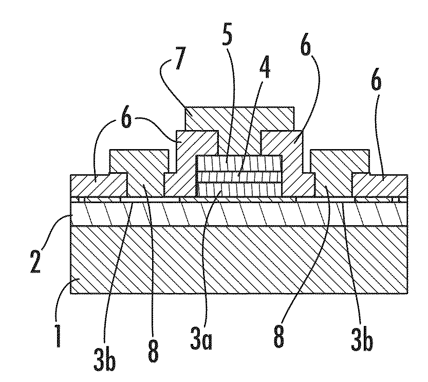
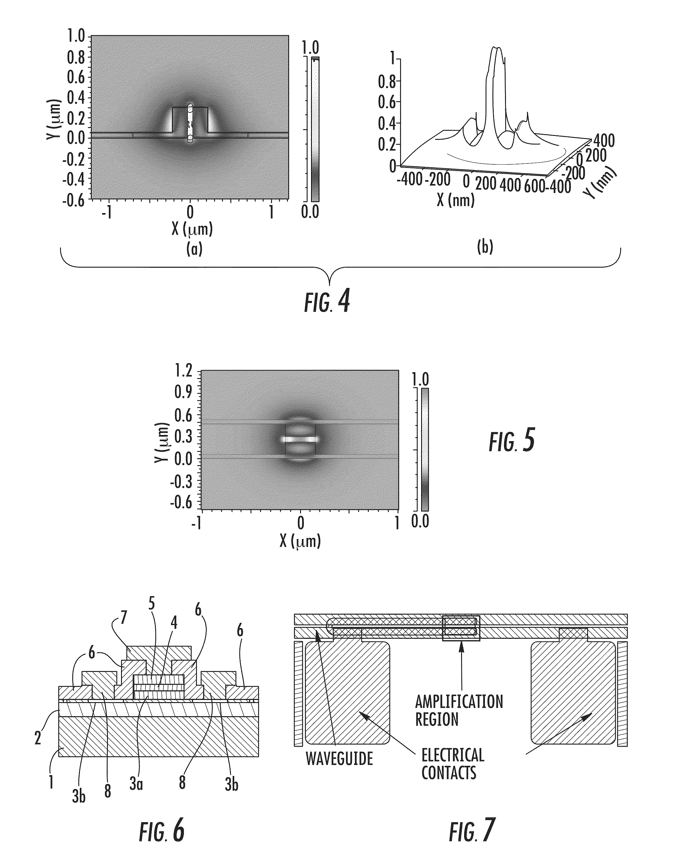
[0047]According to an embodiment, the electroluminescent device comprises a slot waveguide formed of a thin layer of silicon oxide having a relatively low refraction index and thickness smaller that 70 nm, and more preferably 50 nm, between a bottom and a top layer of silicon of a relatively higher refraction index, both of a thickness that may range between 150 nm and 300 nm. At least a portion (tract) between undoped portions of the thin core layer of silicon oxide of the waveguide in the propagation direction of an optical signal, i...


PUM


Abstract

An electrically pumped lateral emission electroluminescent device may include a slotted waveguide including a top silicon layer having a thickness between 150 nm and 300 nm and a refraction index associated therewith, and a bottom silicon layer having a thickness between 150 nm and 300 nm and a refraction index associated therewith. A core layer may include silicon oxide between the top and bottom layers and a thickness less than 70 nm. A core layer refraction index may be greater than each of the top and bottom layer refraction indices. A core layer portion may be in a direction of light propagation and may be doped with erbium, and may include silicon nanocrystals. A portion of each of the top and bottom layers may coincide with the core layer portion and may be doped so that the top and bottom layer portions are electrically conductive to define top and bottom plates.

Description

FIELD OF INVENTION[0001]This invention relates, in general, to the integration of light emitting devices in silicon waveguides for optical signal. This invention also relates to optical waveguide amplifiers that may be integrated in common IC fabrication processes and electrically pumped.BACKGROUND OF THE INVENTION[0002]Based upon technological advances in silicon based microelectronics, integration scales have been reached such that in a 1 cm2 silicon chip there may be billions of transistors and up to 10 km of metal connections. Signal propagation delays, because of parasitic resistors and capacitors (RC) among metal lines and intermetal dielectrics, poses the problem of achieving ever faster signal transmission with relatively small losses. A possible approach is to use optical signal transmission paths. In this way, the signal propagation speed is that of light in the optical medium, e.g. silicon oxide. Moreover a plurality of signals may be simultaneously transmitted through a ...

Claims


Application Information

Patent Timeline
Patent Type & Authority Patents(United States)
IPC IPC(8): H01S5/00
CPCH01S3/0632H01S3/09H01S3/1608H01S3/169H01S3/176H01S3/2308
Inventor CASTAGNA, MARIA ELOISAMUSCARA', ANNA
Owner STMICROELECTRONICS SRL
Why Eureka
Try Eureka