Manufacturing method of monocrystalline silicon and monocrystalline silicon

a manufacturing method and technology of monocrystalline silicon, applied in the direction of crystal growth process, polycrystalline material growth, chemistry apparatus and processes, etc., can solve the problems of inability to perform desired sputtering and the like, and the resistivity during the sputtering or plasma etching process may become different from the target value, so as to improve production efficiency and shorten the time for heating the crucible added with silicon material.

Active Publication Date: 2019-11-26
SUMCO CORP
View PDF6 Cites 1 Cited by
  • Summary
  • Abstract
  • Description
  • Claims
  • Application Information

AI Technical Summary

Benefits of technology

[0029]Since no thermal donor is present in the region held at 650 degrees C. or more for 60 minutes, when the heater 24 is powered off after the holding process and the monocrystalline silicon SM is pulled up while being rapidly cooled to be drawn out of the chamber 21, the time for the straight body SM2 to stay in a temperature range in which the thermal donors are generated (e.g. approximately 450 degrees C.) can be shortened, thereby restraining the generation of the thermal donors to the minimum. It is believed that, consequently, the resistivity of the monocrystalline silicon SM when sputtering or plasma etching process is performed can be restrained from being out of a target value by using the region held at 650 degrees C. or more even without applying the donor-killer heat treatment.
[0048]According to the above arrangement, since the monocrystalline silicon is drawn out after the state holding step while the heater is powered on, and subsequently the silicon material is added in the crucible to manufacture the next monocrystalline silicon, as compared with an instance in which the heater is powered off before the draw-out step, the time for heating the crucible added with the silicon material can be shortened, thereby improving the production efficiency.

Problems solved by technology

However, since the donor-killer heat treatment may sometimes result in a slip dislocation, a method without applying the donor-killer heat treatment has also been studied.
However, according to the method disclosed in Patent Literature 1, it is possible that the resistivity cannot be controlled to be within the range of 10 Ω·cm to 50 Ω·cm due to the thermal hysteresis experienced by the monocrystalline silicon when the monocrystalline silicon is pulled up or uneven oxygen concentration of the monocrystalline silicon, so that the resistivity during the sputtering or plasma etching process may become different from the target value and desired sputtering and the like may be unable to be performed.

Method used


Image

  • Manufacturing method of monocrystalline silicon and monocrystalline silicon
  • Manufacturing method of monocrystalline silicon and monocrystalline silicon
  • Manufacturing method of monocrystalline silicon and monocrystalline silicon

Examples


experiment 1

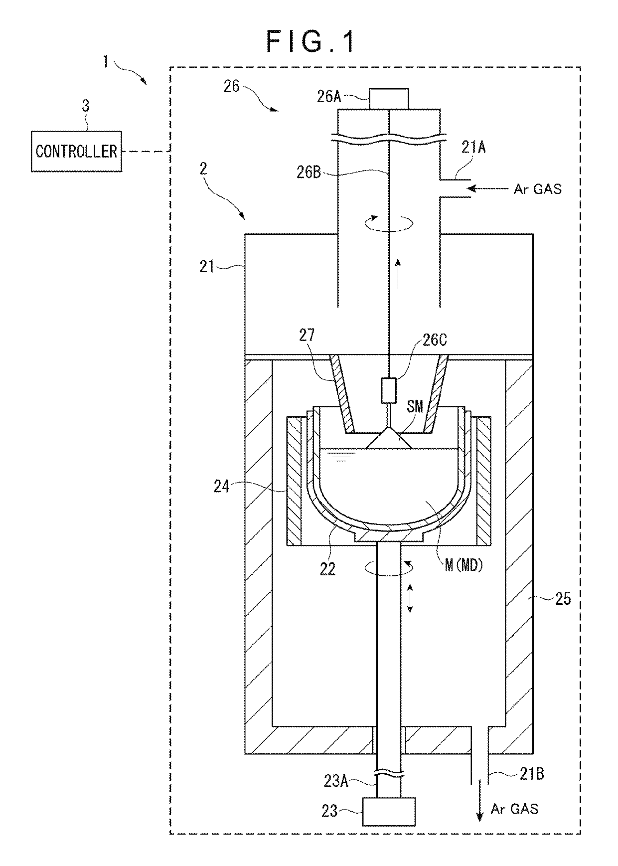
[0084]Initially, the monocrystal pull-up apparatus 1 shown in FIG. 1 was prepared. Then, after performing the same growth step and separating step as those in the exemplary embodiment, the heater was powered off without performing the state holding step, and then the draw-out step was performed. It should be noted that the process for Experiment 1 is the same as a typical process.

experiment 2

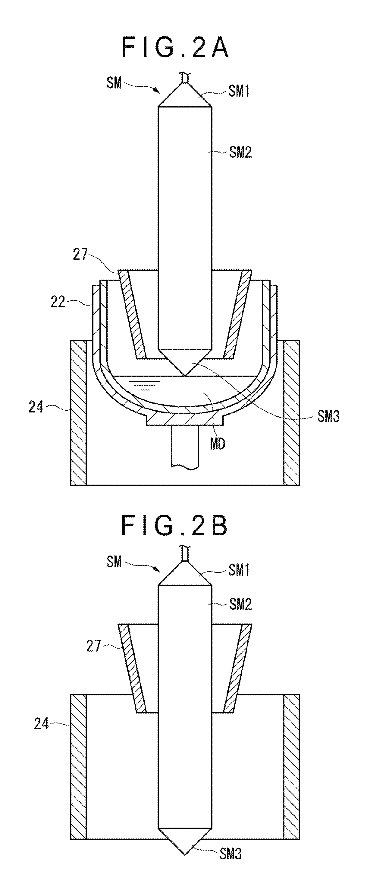
[0085]A monocrystalline silicon was prepared under the same conditions as those in Experiment 1 except that the heater was powered off after the state holding step was performed subsequent to the separating step, and then the draw-out step was performed. During the state holding step, the power of the heater was kept at 60% of the power at the end of the formation of the straight body, and the upper end SM21 of the straight body SM2 was situated at the same level as the upper end 27A of the heat shield 27 as shown in FIG. 5.

Experiments 3, 4

[0086]Monocrystalline silicons were prepared under the same conditions as those in Experiment 2 except that: the upper end of the straight body was located at a vertically middle position in the heat shield in the state holding step (Experiment 3); and the upper end of the straight body was situated at the same level as the lower end of the heat shield (Experiment 4). It should be noted that an experiment using a monocrystalline silicon of 1200 mm...


PUM

PropertyMeasurementUnit
diameteraaaaaaaaaa
resistivityaaaaaaaaaa

Abstract

A manufacturing method of a monocrystalline silicon includes: a growth step in which a seed crystal having contacted a silicon melt is pulled up and a crucible is rotated and raised to form a straight body of the monocrystalline silicon; a separating step in which the monocrystalline silicon is separated from the silicon melt; a state holding step in which the crucible and the monocrystalline silicon are lowered and the monocrystalline silicon is kept at a level at which an upper end of the straight body is located at the same level as an upper end of a heat shield or is located below the upper end of the heat shield for a predetermined time; and a draw-out step in which the monocrystalline silicon is drawn out of a chamber.

Description

[0001]The entire disclosure of Japanese Patent Application No. 2016-101103 filed May 20, 2016 is expressly incorporated by reference herein.TECHNICAL FIELD[0002]The present invention relates to a manufacturing method of a monocrystalline silicon, and a monocrystalline silicon.BACKGROUND ART[0003]In general, monocrystalline silicon grown by Czochralski process (CZ process) includes thermal donors derived from interstitial oxygen. The thermal donors are generated depending on a thermal hysteresis experienced by the monocrystalline silicon when the monocrystalline silicon is pulled up, where it is known that the thermal donors are generated on a section of a straight body near an upper end thereof but are not generated on a section of the straight body near a lower end thereof. When there are thermal donors in the monocrystalline silicon used for a target material of sputtering or a plasma etching electrode, the resistivity of the monocrystalline silicon during the sputtering or plasma...

Claims


Application Information

Patent Timeline
Patent Type & Authority Patents(United States)
IPC IPC(8): C30B15/14H01L21/02C30B29/06H01L21/033H01L21/263H01L21/67H01L21/60
CPCH01L21/02008C30B15/14C30B29/06H01L21/02H01L21/0334H01L21/2636H01L21/67011H01L2021/60202
Inventor NAKAMURA, TSUYOSHIKAWASAKI, EIICHIKOBAYASHI, SHOGOOSHIRO, YOSHIHIRO
Owner SUMCO CORP
Why Eureka
Try Eureka