Electro-optical device and electronic apparatus with sampling and monitoring transistors

a technology of optical devices and electronic devices, applied in the direction of semiconductor devices, optics, instruments, etc., can solve the problems of unstable operation cracks in the insulating film, and the failure of the sample and hold circuit to operate properly, etc., to achieve stable operation and high reliability quality

Active Publication Date: 2019-12-03
SEIKO EPSON CORP
View PDF15 Cites 1 Cited by
  • Summary
  • Abstract
  • Description
  • Claims
  • Application Information

AI Technical Summary

Benefits of technology

[0015]According to the application example, by constituting the sampling transistor with a plurality of transistors, a gap generated between the sampling transistors disposed adjacently in accordance with the disposition of the data lines is not continuous in the direction in which the plurality of transistors are disposed, that is, the channel width direction. Therefore, even though a stress due to, for example, heat or the like acts on the insulating film filling the gap, the stress easily disperses, and cracks due to the stress are hardly generated in the insulating film filling the gap. Thus, it is possible to prevent the occurrence of a problem that cracks grow and lead to the semiconductor layer or a wiring connected to the semiconductor layer, so that the sample and hold circuit does not operate properly.
[0016]On the other hand, since the monitoring transistor of the monitor circuit is not made of a plurality of transistors like a sampling transistor but is made of one transistor, the monitoring transistor is hardly affected by a variation depending on the manufacturing process of the transistor. Since the monitoring transistor is unnecessary to be disposed in accordance with the disposition of the data lines like the sampling transistor, it is possible to adjust a gap such that cracks are hardly generated in the insulating film filling the gap between the adjacent monitoring transistors. That is, it is possible to provide an electro-optical device in which a sampling transistor and a monitoring transistor are appropriately disposed to obtain a stable driving state.
[0021]According to this configuration, it is easy to further disperse the stress due to, for example, heat or the like applied to the insulating film filling the gap between the adjacent sampling transistors. That is, cracks due to the stress are hardly generated in the insulating film filling the gap.
[0029]According to this configuration, the threshold characteristics of the monitoring transistor are not excessively enhanced.
[0033]According to this configuration, even though the disposition pitch of pixels, that is, the disposition pitch of data lines becomes narrow, it is possible to dispose the sampling transistors at a narrow pitch correspondingly. Since monitoring transistors may be also disposed at a narrow pitch, it is possible to reduce a region in which monitor circuits are disposed. In addition, since the gate lines are linear, it is easy to pattern the gate lines, and it is possible to suppress the variation of the width of the gate electrode, that is, substantially, the channel length of each transistor.Application Example 2
[0035]According to the application example, it is possible to provide an electronic apparatus including an electro-optical device having stable operation and high reliability quality.

Problems solved by technology

Therefore, in a case where the widths of gate electrodes vary due to meandering, a channel length in a semiconductor layer opposite to the gate electrodes substantially varies, and there is a possibility that the operations of the sample and hold circuit become unstable.
Since an insulating film composed of a material different from the material of the semiconductor layer is present in the space, there is a possibility that a stress is applied to the space to cause cracks in the insulating film, for example, in a case where heat treatment or the like is performed in the manufacturing process of the active matrix substrate.
In a case where cracks grow and lead to the semiconductor layer or the wiring connected to the semiconductor layer, there is a possibility that a problem that the sample and hold circuit does not operate properly will occur.
Therefore, even though a stress due to, for example, heat or the like acts on the insulating film filling the gap, the stress easily disperses, and cracks due to the stress are hardly generated in the insulating film filling the gap.
Thus, it is possible to prevent the occurrence of a problem that cracks grow and lead to the semiconductor layer or a wiring connected to the semiconductor layer, so that the sample and hold circuit does not operate properly.
That is, cracks due to the stress are hardly generated in the insulating film filling the gap.

Method used


Image

  • Electro-optical device and electronic apparatus with sampling and monitoring transistors
  • Electro-optical device and electronic apparatus with sampling and monitoring transistors
  • Electro-optical device and electronic apparatus with sampling and monitoring transistors

Examples


first embodiment

Electro-Optical Device

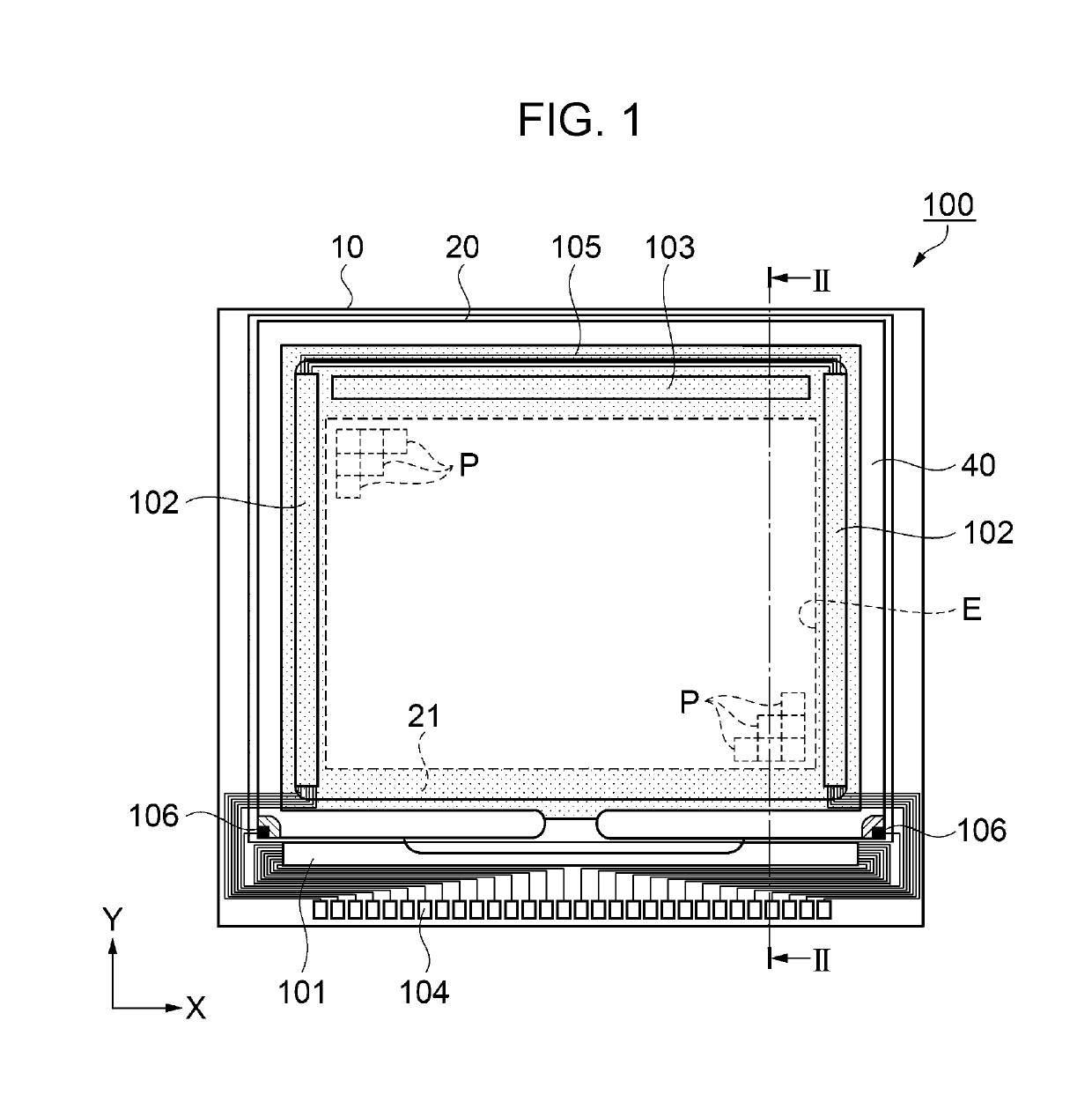
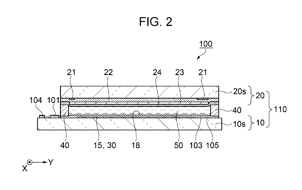
[0064]First, a schematic configuration of a liquid crystal device as an electro-optical device of this embodiment will be described with reference to FIGS. 1 and 2. FIG. 1 is a schematic plan view showing a configuration of a liquid crystal device, and FIG. 2 is a schematic sectional view taken along the line II-II of the liquid crystal device shown in FIG. 1.

[0065]As shown in FIGS. 1 and 2, a liquid crystal device 100 as an electro-optical device of this embodiment includes an element substrate 10 and an opposing substrate 20 that are disposed opposite to each other, and a liquid crystal layer 50 sandwiched between the pair of substrates. For the base material 10s of the element substrate 10 and the base material 20s of the opposite substrate 20, for example, a transparent quartz substrate or a glass substrate are used.

[0066]The element substrate 10 is slightly larger than the opposite substrate 20, both substrates are adhered via a sealing material 40 dispose...

modification example 1

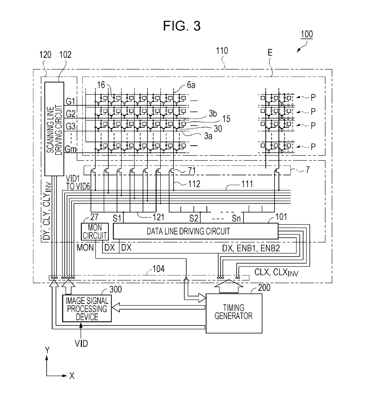
[0143]As shown in FIG. 14, the sample and hold (SH) circuit 7 of Modification Example 1 includes the sampling transistors (S-TFT) 71 made of a plurality of (four) transistors 71A, 71B, 71C, and 71D aligned in the Y direction in which a linear gate line 71g extends, and connected in parallel. Under the layer of the plurality of transistors 71A, 71B, 71C, and 71D, a light shielding layer 76 divided for each of the plurality of transistors 71A, 71B, 71C, and 71D in the Y direction is provided. The channel widths in the plurality of transistors 71A, 71B, 71C, and 71D and the width L4 of the divided light shielding layer 76 in the Y direction are about 150 μm as described above. The SH circuit 7 and the light shielding layer 76 are provided on the element substrate 10.

[0144]As shown in FIG. 15, the light shielding layer 76 is divided in a state of straddling three transistors in the X direction. The light shielding layer 76 is divided such that the division position of the light shieldin...

modification example 2

[0150]As shown in FIG. 18, the sample and hold (SH) circuit 7 of Modification Example 2 includes the sampling transistors (S-TFT) 71 made of a plurality of (four) transistors 71A, 71B, 71C, and 71D aligned in the Y direction in which a linear gate line 71g extends and connected in parallel. Under the layer of a plurality of transistors 71A, 71B, 71C, and 71D, a light shielding layer 77 divided for each of the plurality of transistors 71A, 71B, 71C, and 71D in the Y direction is provided. The channel widths in the plurality of transistors 71A, 71B, 71C and 71D, and the width L4 of the divided light shielding layer 77 in the Y direction are about 150 μm as described above. The SH circuit 7 and the light shielding layer 77 are provided on the element substrate 10.

[0151]The light shielding layer 77 is disposed so as to overlap two transistors (the semiconductor layer 70a) adjacent in the X direction, and has portions that protrude in the X direction, corresponding to the source contact ...


PUM

PropertyMeasurementUnit
lengthaaaaaaaaaa
lengthaaaaaaaaaa
widthaaaaaaaaaa

Abstract

An electro-optical device (e.g., a liquid crystal device) includes a data line connected to a switching element provided for each pixel, a sampling transistor that has a gate supplied with a selection signal, a source supplied with an image signal, and a drain connected to the data line, and a monitoring transistor. A gate of the monitoring transistor is supplied with an input signal. A delay signal indicating a delay amount of the selection signal is sent out from a drain of the monitoring transistor. The sampling transistor includes a plurality of transistors connected in parallel to each other along the data line. The monitoring transistor includes one transistor along the data line.

Description

BACKGROUND1. Technical Field[0001]The present invention relates to an electro-optical device and an electronic apparatus including the electro-optical device.2. Related Art[0002]There is disclosed an active matrix type liquid crystal display device as an electro-optical device, including a sample and hold circuit for supplying a plurality of phase-developed image signals to sequentially selected data lines, and a precharge circuit that supplies image auxiliary input signals to the data lines before the application of image signals by the sample and hold circuit during one horizontal retrace period (JP-A-2003-177376).[0003]In the active matrix type liquid crystal display device of JP-A-2003-177376, in signal transmission paths for transmitting signals from a plurality of image signal lines to a desired sample and hold circuit through relay wirings, the relay wirings made of a conductive film having a higher resistance than the image signal lines, are formed to have the same width and...

Claims


Application Information

Patent Timeline
Patent Type & Authority Patents(United States)
IPC IPC(8): G02F1/1362H01L27/12G02F1/1335G02F1/1345G02F1/1368H01L29/786G02F1/133G02F1/1343
CPCG02F1/133512G02F1/1343G02F1/13454G02F1/136286G02F1/13306H01L29/78633H01L29/78675H01L27/1222G02F2201/123G02F1/136209G02F2001/13685G02F1/13685
Inventor NAGASAWA, HITOYA
Owner SEIKO EPSON CORP
Why Eureka
Try Eureka