Column-dependent positive voltage boost for memory cell supply voltage

Active Publication Date: 2019-12-31
GLOBALFOUNDRIES US INC
View PDF12 Cites 1 Cited by
  • Summary
  • Abstract
  • Description
  • Claims
  • Application Information

AI Technical Summary

Benefits of technology

The patent describes an integrated circuit chip that includes a memory array and a positive voltage boost circuit (PVBC) to improve the writeability of memory cells. The PVBC provides boosted voltage pulses to the memory cells during write operations, while the chip operates at a relatively low voltage. The method includes applying the boost pulses to selected columns in the array to minimize power consumption. The chip can be manufactured and tested to identify which process corners it operates at and which groups of chips would benefit from the PVBC. The technical effect is to improve the speed and reliability of writing data to memory cells in the chip, even at low operating voltages.

Problems solved by technology

Those skilled in the art will recognize that the combination of memory cell size scaling, positive cell supply voltage (PVCS) lowering, and process variations can cause memory cell writeability issues.
However, if the second pull-up transistor 111 is not turned off fast enough and the first pull-up transistor 101 is not turned on fast enough, because of insufficient headroom at lower voltages, then the voltage on the storage node true 105 may not rise to the PVCS level such that the write is not completed.
An incomplete write will make the cell unstable in subsequent read operations.

Method used


Image

  • Column-dependent positive voltage boost for memory cell supply voltage
  • Column-dependent positive voltage boost for memory cell supply voltage
  • Column-dependent positive voltage boost for memory cell supply voltage

Examples


Embodiment Construction

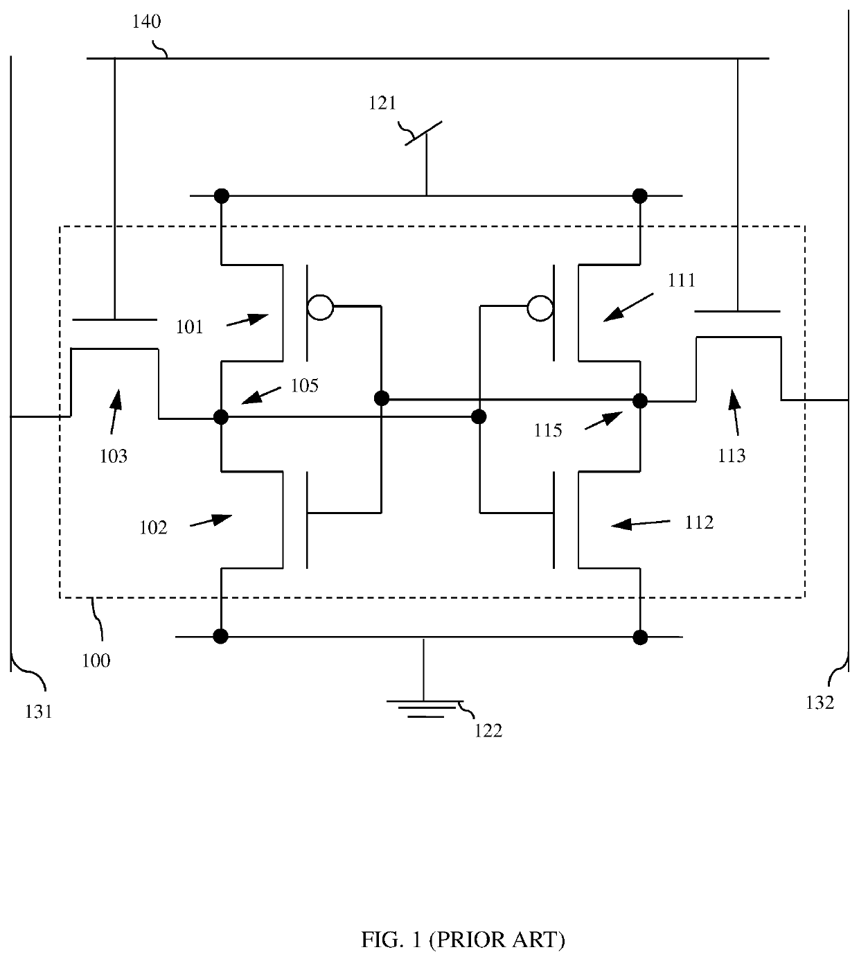
[0026]As mentioned above, for a static random access memory (SRAM) cell 100, such as that shown in FIG. 1, the combination of size scaling (e.g., using single semiconductor fin pull-up transistors), positive cell supply voltage (PVCS) lowering and process variations (e.g., threshold voltage variations at the process corners) can result in some pull-up transistors 101, 111 across the memory array with insufficient headroom to ensure that a data value is stored properly on the storage node during the write operation. Specifically, when writing a “1” data value to the storage node true 105, the bitline true 131 remains charged to the PVCS level and the bitline complement 132 is discharged to ground 122. When the wordline is activated, the voltage level on the storage node true 105 increases. To ensure that the data value of “1” is stored on the storage node true 105, the voltage on this storage node true 105 needs to rise to the PVCS level and remain there. However, if the second pull-...


PUM


Abstract

Disclosed is a chip with a memory array and at least one positive voltage boost circuit, which provides positive voltage boost pulses to the sources of pull-up transistors in the memory cells of the array during write operations to store data values in those memory cells and, more specifically, provides positive voltage boost pulses substantially concurrently with wordline deactivation during the write operations to ensure that the data is stored. Application of such pulses to different columns can be performed using different positive voltage boost circuits to minimize power consumption. Also disclosed are a memory array operating method that employs a positive voltage boost circuit and a chip manufacturing method, wherein post-manufacture testing is performed to identify chips having memory arrays that would benefit from positive voltage boost pulses and positive voltage boost circuits are attached to those identified chips and operably connected to the memory arrays.

Description

BACKGROUNDField of the Invention[0001]The present invention relates to memory arrays (e.g., static random access memory (SRAM) arrays) and, more particularly, to integrated circuit (IC) structures with memory arrays and methods of manufacturing and operating such IC structures to enhance low voltage writeability.Description of Related Art[0002]Those skilled in the art will recognize that the combination of memory cell size scaling, positive cell supply voltage (PVCS) lowering, and process variations can cause memory cell writeability issues.[0003]For example, FIG. 1 is a schematic drawing illustrating a conventional six-transistor (6T) static random access memory (SRAM) cell 100, which includes a pair of complementary storage nodes (i.e., storage node true 105 and storage node complement 115) and which is connected to a wordline (WL) 140 and to a pair of complementary bitlines (i.e., bitline true 131 and bitline complement 132) within an SRAM memory array (not shown). Specifically, ...

Claims


Application Information

Patent Timeline
IPC IPC(8): G11C11/00G11C11/412G11C11/419
CPCG11C11/419G11C11/412G11C5/145G11C7/12
Inventor BRINGIVIJAYARAGHAVAN, VENKATRAGHAVANPOTLADHURTHI, ESWARARAOBRACERAS, GEORGE M.
Owner GLOBALFOUNDRIES US INC
Why Eureka
Try Eureka