Protection schemes for MEMS switch devices

a technology of protection schemes and switch devices, applied in emergency protective arrangements, relays, coatings, etc., can solve problems such as electrical over-stress in the power supply of the switch device, and achieve the effect of reducing the risk of over-stress in the power supply devi

Active Publication Date: 2020-01-07
ANALOG DEVICES INT UNLTD
View PDF26 Cites 3 Cited by
  • Summary
  • Abstract
  • Description
  • Claims
  • Application Information

AI Technical Summary

Benefits of technology

[0006]Micro-electromechanical (MEMS) switch devices can be fabricated using integrated circuit fabrication techniques and materials. Such switch devices can provide cycle life and insertion loss performance suiting a broad range of applications including, for example, automated test equipment (ATE), switching for measurement instrumentation (such as a spectrum analyzer, network analyzer, or communication test system), and uses in communication systems, such as for signal processing. MEMS devices can be vulnerable to electrical over-stress, such as associated with electrostatic discharge (ESD) transient events or other transient overvoltage conditions. A solid-state clamp circuit can be incorporated in a MEMS device package to protect one or more MEMS devices from damaging overvoltage conditions. The clamp circuit can be monolithically integrated with a MEMS device using a commonly-shared substrate, or the clamp circuit can be heterogeneously integrated and be formed on a separate substrate. The clamp circuit can include single or multiple blocking junction structures having complementary current-voltage relationships, such as to help linearize a capacitance-to-voltage relationship presented by the clamp circuit.
[0008]In an example, a method can include providing an electronic circuit having a micro-electromechanical switch device and a solid-state clamp circuit using a commonly-shared integrated circuit device package. The method can include forming an integrated micro-electromechanical switch device upon or within a first substrate, forming a hermetic enclosure defining a hermetically isolated region to isolate the integrated micro-electromechanical switch device from a surrounding environment, the hermetic enclosure comprising a dielectric material, forming a solid-state clamp circuit, and electrically coupling the solid-state clamp circuit to the micro-electromechanical switch to suppress or inhibit damage to the micro-electromechanical switch due to a transient overvoltage condition.

Problems solved by technology

MEMS devices can be vulnerable to electrical over-stress, such as associated with electrostatic discharge (ESD) transient events or other transient overvoltage conditions.

Method used


Image

  • Protection schemes for MEMS switch devices
  • Protection schemes for MEMS switch devices
  • Protection schemes for MEMS switch devices

Examples


Embodiment Construction

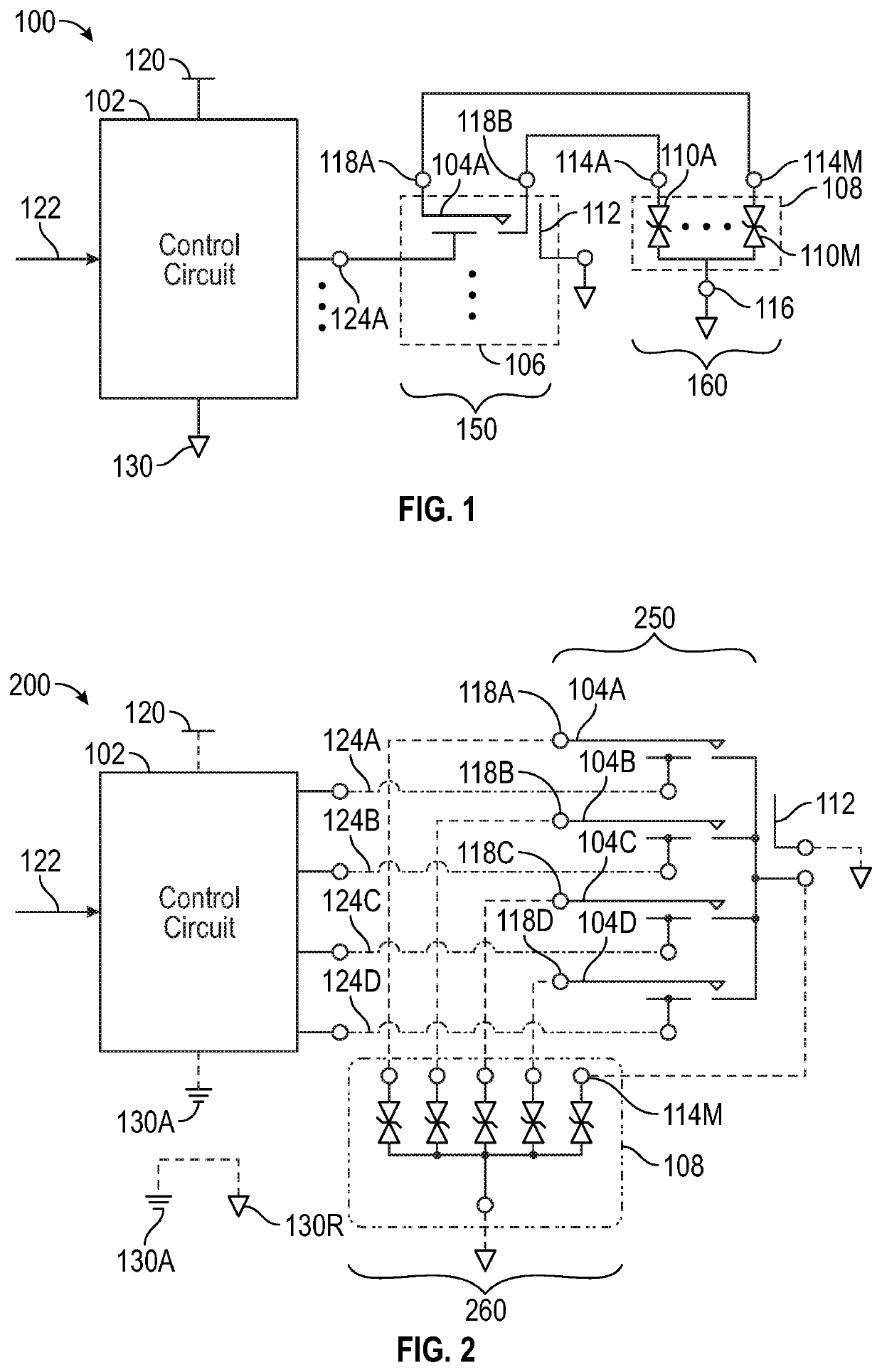
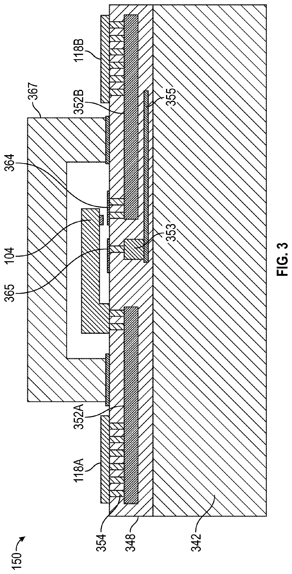
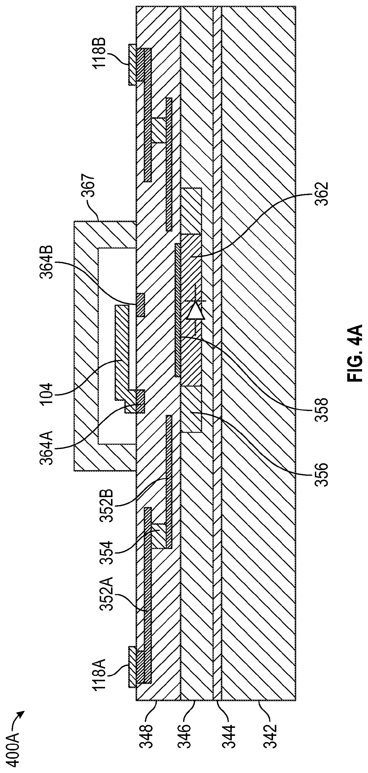
[0037]As mentioned above, micro-electromechanical (MEMS) switch devices can be fabricated using integrated circuit fabrication techniques and materials. Such switch devices can provide insertion and return loss performance suitable for use in a broad range of applications. Micro-electromechanical devices are used more generally in other non-switching applications such as for gyroscopes or accelerometers. But, in such motion or position sensing applications, the micro-electromechanical device is generally not exposed to an “interface environment” where damaging voltages could be applied to the micro-electromechanical device terminals.

[0038]By contrast, the present inventors have recognized, among other things, that in certain applications, the terminals of such MEMS devices can be electrically exposed to an environment outside the integrated circuit device package through an interface, and are thereby more vulnerable to electrical over-stress, particularly damaging overvoltage transi...


PUM

PropertyMeasurementUnit
frequencyaaaaaaaaaa
frequencyaaaaaaaaaa
voltageaaaaaaaaaa

Abstract

Micro-electromechanical switch (MEMS) devices can be fabricated using integrated circuit fabrication techniques and materials. Such switch devices can provide cycle life and insertion loss performance suiting for use in a broad range of applications including, for example, automated test equipment (ATE), switching for measurement instrumentation (such as a spectrum analyzer, network analyzer, or communication test system), and uses in communication systems, such as for signal processing. MEMS devices can be vulnerable to electrical over-stress, such as associated with electrostatic discharge (ESD) transient events. A solid-state clamp circuit can be incorporated in a MEMS device package to protect one or more MEMS devices from damaging overvoltage conditions. The clamp circuit can include single or multiple blocking junction structures having complementary current-voltage relationships, such as to help linearize a capacitance-to-voltage relationship presented by the clamp circuit.

Description

FIELD OF THE DISCLOSURE[0001]This document pertains generally, but not by way of limitation, to integrated micro-electromechanical switch devices and protection circuits coupled thereto.BACKGROUND[0002]Electrical transients can cause damage to electronic circuits. Such transients can be induced in relation to electrostatic discharge (ESD) events, where bound electric charge can develop significant potentials, such as in excess of 1 kiloVolt (kV) relative to a reference potential. Stored charge can be accumulated through, for example, triboelectric effect (e.g., contact electrification) in relation to ungrounded personnel or equipment, or even induced by proximity to other charged objects. If a discharge path is presented, such as by contact between the personnel or equipment and a sensitive device, the stored charge can be coupled to the sensitive device and discharged through the sensitive device, such as inducing a damaging transient overvoltage condition.[0003]Certain electronic ...

Claims


Application Information

Patent Timeline
Patent Type & Authority Patents(United States)
IPC IPC(8): H02H9/00B81C1/00H02H9/04H01L23/31H01H59/00H01L27/02H01L23/495H01L27/12
CPCH01L27/0262B81C1/00246H02H9/046H01L23/3107H01H59/0009B81C1/0023H02H9/041H01L27/0255H01L2924/181H01L2224/48227H01L2224/48247H01L2224/48137H01L2924/16235H01L2924/00012B81C2203/0735H01L2924/19105H01L27/1203H01L2224/48091H01L23/49541H01L2224/48145H01L2924/00014B81B7/0064B81B7/008
Inventor FITZGERALD, PADRAIG LIAMPARTHASARATHY, SRIVATSANSALCEDO, JAVIER A.
Owner ANALOG DEVICES INT UNLTD
Why Eureka
Try Eureka