Alignment mark and measurement method thereof

a technology of alignment mark and measurement method, which is applied in the direction of semiconductor/solid-state device testing/measurement, instruments, photomechanical equipment, etc., can solve the problems of inaccurate measurement results, inability to accurately reflect the real position of the relative position between successive layers, and still have some drawbacks of current overlay measurement, so as to reduce the dishing phenomenon and improve the accuracy of the alignment step

Active Publication Date: 2020-02-18
UNITED MICROELECTRONICS CORP
View PDF8 Cites 3 Cited by
  • Summary
  • Abstract
  • Description
  • Claims
  • Application Information

AI Technical Summary

Benefits of technology

[0008]One feature of the present invention is that plurality of dummy alignment marks are added in the blank region. In this way, it is possible to reduce the dishing phenomenon caused by the blank region when the planarization step is performed. Therefore, if other alignment marks are formed in other layer structures to overlap the blank region, the accuracy of the alignment step can be improved.

Problems solved by technology

However, the current overlay measurement still has some drawbacks.
For example, due to measurement deviation, the measured values of relative positions between successive layers often fail to reflect their real positions.
Therefore, the measurement results often include overlay error.

Method used


Image

  • Alignment mark and measurement method thereof
  • Alignment mark and measurement method thereof
  • Alignment mark and measurement method thereof

Examples


Embodiment Construction

[0021]In the following description, numerous specific details are given to provide a thorough understanding of the invention. It will, however, be apparent to one skilled in the art (note: of ordinary skill in the art) that the invention may be practiced without these specific details. Furthermore, some well-known system configurations and process steps are not disclosed in detail, as these should be well-known to those skilled in the art.

[0022]Likewise, the drawings showing embodiments of the apparatus are not to scale and some dimensions are exaggerated for clarity of presentation. Also, where multiple embodiments are disclosed and described as having some features in common, like or similar features will usually be described with same reference numerals for ease of illustration and description thereof.

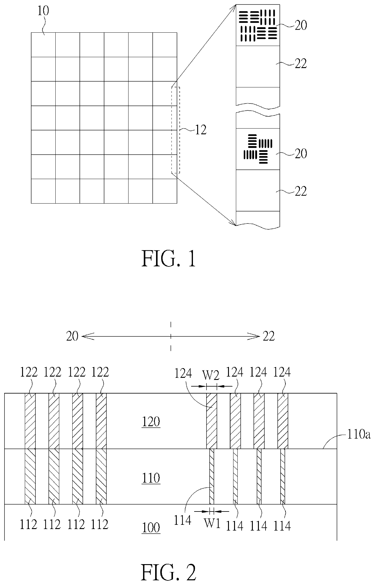
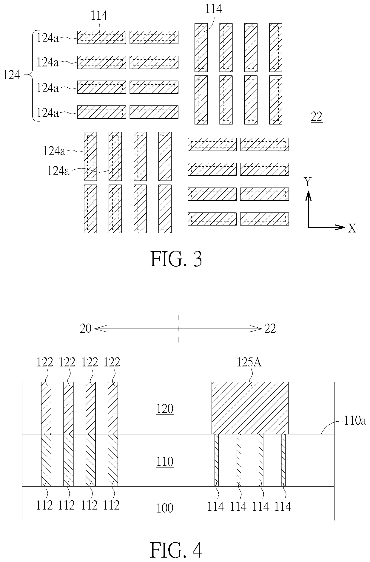
[0023]Firstly, please refer to FIG. 1, the present invention provides an alignment mark. This alignment mark is often set in a scribe line 12 of a wafer 10. It is noteworthy that in...


PUM

PropertyMeasurementUnit
sizeaaaaaaaaaa
widthaaaaaaaaaa
shapeaaaaaaaaaa

Abstract

The present invention provides an alignment mark, the alignment mark includes at least one dummy mark pattern in a first layer comprises a plurality of dummy mark units arranged along a first direction, and at least one first mark pattern located in a second layer disposed above the first layer, the first mark pattern comprises a plurality of first mark units, each of the first mark units being arranged in a first direction. When viewed in a top view, the first mark pattern completely covers the dummy mark pattern, and the size of each dummy mark unit is smaller than each first mark unit. In addition, each dummy mark unit of the dummy mark pattern has a first width, each first mark unit of the first mark pattern has a second width, and the first width is smaller than half of the second width.

Description

BACKGROUND OF THE INVENTION1. Field of the Invention[0001]The present invention relates to semiconductor processes a field, and more particularly to an alignment mark and a measurement method thereof.2. Description of the Prior Art[0002]Photolithography is an essential step in semiconductor manufacturing processes, through which the pattern of integrated circuits may be transferred from photomasks to semiconductor chips. Generally, a design layout of integrated circuit provided by an IC design house may be divided into several layers of design layouts after it is received by the semiconductor manufacturing company. These design layouts may be then fabricated on the corresponding transparent plates to thereby form photomasks with desired layouts. The layout of each of the photomasks may be respectively transferred to a photoresist layer on the chip through suitable photolithographic process. Afterwards, other suitable processes, such as etching, deposition, doping, CMP, thermal / annea...

Claims


Application Information

Patent Timeline
Patent Type & Authority Patents(United States)
IPC IPC(8): H01L23/544G03F9/00G01B21/20G03F7/20G01B21/24H01L21/66
CPCG03F7/70633G03F9/7073G01B21/24H01L23/544H01L22/12G01B21/20H01L2223/5446G01B2210/56H01L2223/5442H01L2223/54426
Inventor SUN, CHIA-CHENTUNG, YU-CHENGHSUEH, SHENG-YUANLIN, FAN-WEI
Owner UNITED MICROELECTRONICS CORP
Why Eureka
Try Eureka