
Analog switches immune to power sequence

a technology of analog switches and power sequences, applied in the field of computing systems, can solve the problems of unsatisfactory current flows through the parasitic diode, increase power consumption, forward bias currents increase power consumption, etc., and achieve the effect of preventing forward biasing of the parasitic diod

Active Publication Date: 2020-02-18
APPLE INC
View PDF12 Cites 0 Cited by
  • Summary
  • Abstract
  • Description
  • Claims
  • Application Information

AI Technical Summary

Benefits of technology

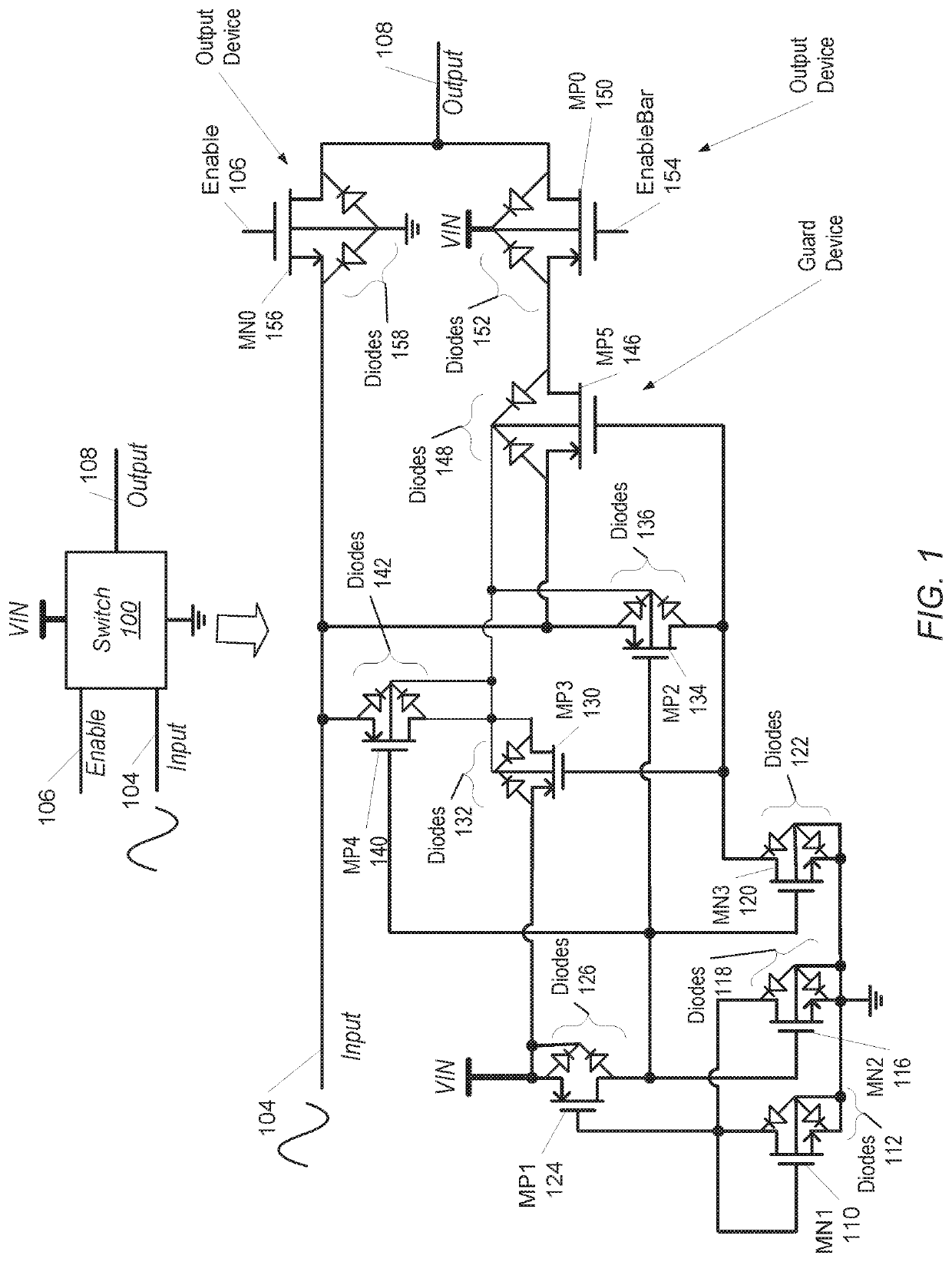
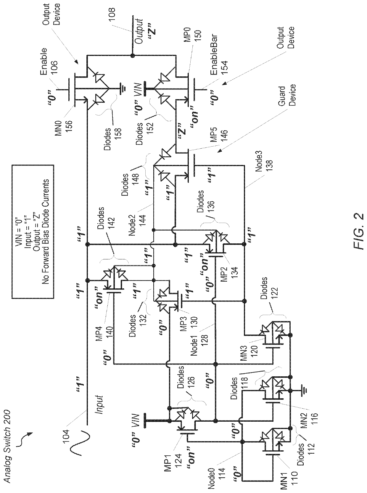
The patent text describes a circuit design that prevents a logic high level or a logic low level from being driven on the output p-type device. The circuit includes a given switch and a guard p-type device in series with the output p-type device. The guard p-type device receives the input signal and is disabled when the input signal is greater than its threshold voltage, which prevents driving a logic high level or a logic low level on the output p-type device. This prevents the parasitic diode of the output p-type device from being forward biased and avoids any parasitic diode current flow. The given switch also includes other devices to ensure the body terminal of the guard p-type device is driven to a logic high level regardless of the voltage levels on the input signal and the power supply signal. The technical effect of this circuit design is to prevent damage to the output p-type device and improve the stability of the circuit.

Problems solved by technology

Due to the fabrication methods of the two types of devices used in CMOS switches, the devices include parasitic diodes.
When this parasitic diode is forward biased, undesirable current flows through the parasitic diode.
The undesirable current increases power consumption.
The forward bias currents increase power consumption.

Method used


Image

  • Analog switches immune to power sequence
  • Analog switches immune to power sequence
  • Analog switches immune to power sequence

Examples


Embodiment Construction

[0025]In the following description, numerous specific details are set forth to provide a thorough understanding of the embodiments described in this disclosure. However, one having ordinary skill in the art should recognize that the embodiments might be practiced without these specific details. In some instances, well-known circuits, structures, and techniques have not been shown in detail for ease of illustration and to avoid obscuring the description of the embodiments.

[0026]Turning now to FIG. 1, a block diagram illustrating one embodiment of an analog switch 100 is shown. In various embodiments, the analog switch 100 receives an analog input signal 104, and when enabled, conveys the received input signal 104 as the output signal 108 as an analog signal. The analog switch 100 also receives a power supply voltage (or power supply signal) designated as “VIN” as well as a ground reference voltage level. The power supply voltage VIN is also referred to as the power supply signal VIN ...


PUM


Abstract

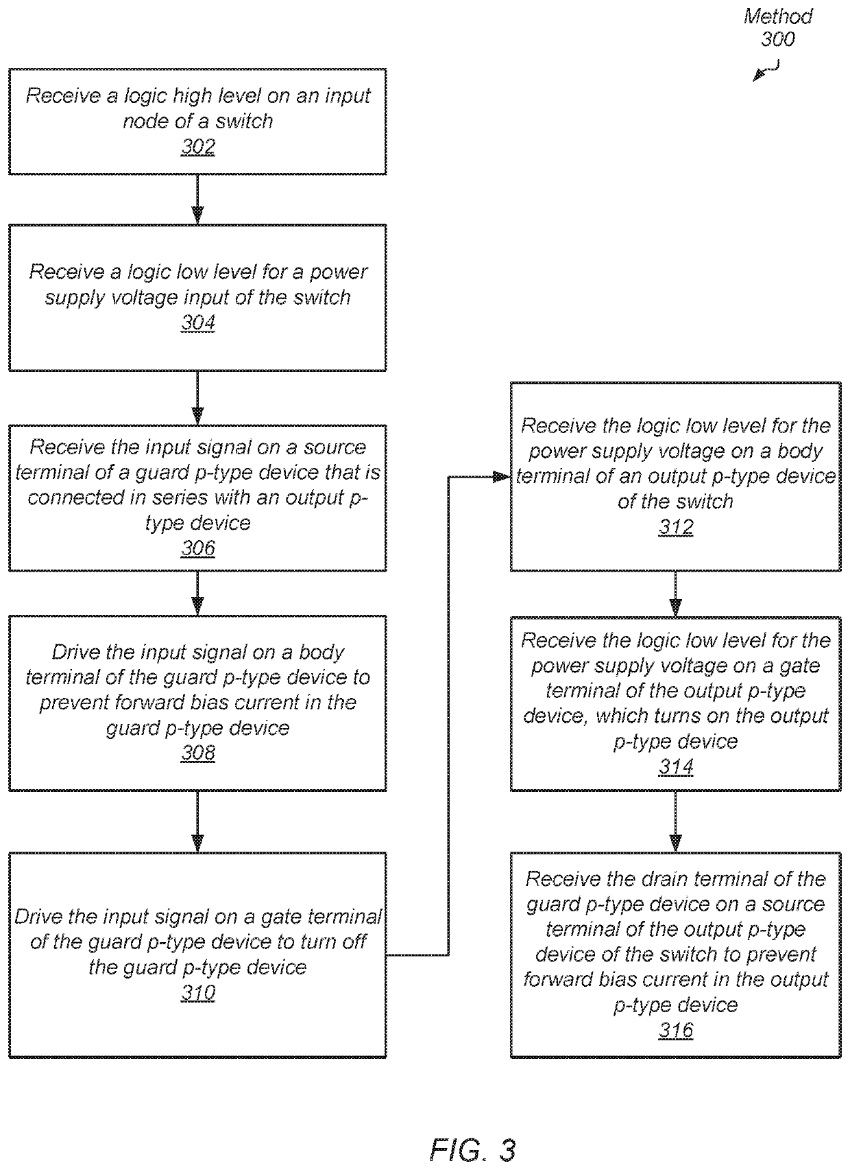
A system and method for efficiently receiving analog input signals. In various embodiments, a functional unit includes a switch in its interface logic. The switch receives an analog input signal, and when enabled, conveys the received input signal as an analog output signal. The switch is enabled when the received enable signal is asserted. However, when the power supply voltage is at a logic low level, an output n-type device is disabled while an output p-type device is enabled. A guard p-type device serially connected with the output p-type device is disabled by other devices used to control the guard p-type device. The control devices also ensure that the body terminals of the guard p-type device and other p-type devices receive a logic high level regardless of the power supply value, which prevents forward bias currents in parasitic diodes of the p-type devices.

Description

BACKGROUNDTechnical Field[0001]Embodiments described herein relate to the field of computing systems and, more particularly, to efficiently receiving analog input signals.Description of the Related Art[0002]A computing system such as a semiconductor chip includes multiple functional blocks or units, each capable of processing data. In various embodiments, the multiple functional units are individual dies on one of a system on a chip (SOC), a multi-chip module (MCM) or a printed circuit board. Examples of functional units are general-purpose processors with one or more cores in a central processing unit (CPU), highly parallel data architected processors with one or more cores in graphics processing units (GPUs) and digital signal processors (DSPs), display controllers, audio processing components, a camera processing unit, networking components, peripheral interface controllers, memory controllers, and so on.[0003]Control logic, such as a power management unit, within the computing s...

Claims


Application Information

Patent Timeline
IPC IPC(8): H03K19/0185G06F1/324G06F1/3296H03K19/00H03K5/08
CPCH03K5/08H03K19/0013H03K19/018521G06F1/324G06F1/3296G06F1/32Y02D10/00
Inventor ZHANG, WEIBIAO
Owner APPLE INC
Learn More