Flexible organic light emitting diode display with directional crystallized channel and manufacturing method thereof

a light-emitting diode and flexible technology, applied in the field of flexible organic light-emitting diode display and manufacturing method thereof, can solve the problems of device failure, deterioration of electrical characteristics of tft, etc., and achieve the effect of improving the reliability of tft, and improving the reliability of flexible display devi

Active Publication Date: 2020-02-25
WUHAN CHINA STAR OPTOELECTRONICS TECH CO LTD
View PDF11 Cites 0 Cited by
  • Summary
  • Abstract
  • Description
  • Claims
  • Application Information

AI Technical Summary

Benefits of technology

An object of the present disclosure is to provide a flexible organic light emitting diode display and manufacturing method thereof, by which a grain boundary density of an LTPS film along a lengthwise direction of a channel can be decreased.
In the flexible organic light emitting diode display and manufacturing method of the present disclosure, since the active layer is made by the oriented crystalline polycrystalline silicon film, the grain boundary density of the LTPS thin film along the TFT channel direction is low. Therefore, the TFT has better electrical properties, and an inter-granular fracture / deformation does not easily occur at a grain boundary under a bending stress, thereby increasing a reliability of the TFT and increasing a reliability of the flexible display device under bending stress.

Problems solved by technology

Since an atomic binding force at a crystalline interface of the LTPS thin film is weak, an inter-granular fracture / deformation occurs at the grain boundary under a bending stress, so that electrical characteristics of the TFT are deteriorated and the device even fails.

Method used


Image

  • Flexible organic light emitting diode display with directional crystallized channel and manufacturing method thereof
  • Flexible organic light emitting diode display with directional crystallized channel and manufacturing method thereof
  • Flexible organic light emitting diode display with directional crystallized channel and manufacturing method thereof

Examples


Embodiment Construction

The following embodiments refer to the accompanying drawings for exemplifying specific implementable embodiments of the present disclosure. Moreover, directional terms described by the present disclosure, such as upper, lower, front, back, left, right, inner, outer, side, etc., are only directions by referring to the accompanying drawings, and thus the used directional terms are used to describe and understand the present disclosure, but the present disclosure is not limited thereto. In the drawings, the same reference symbol represents the same or similar components.

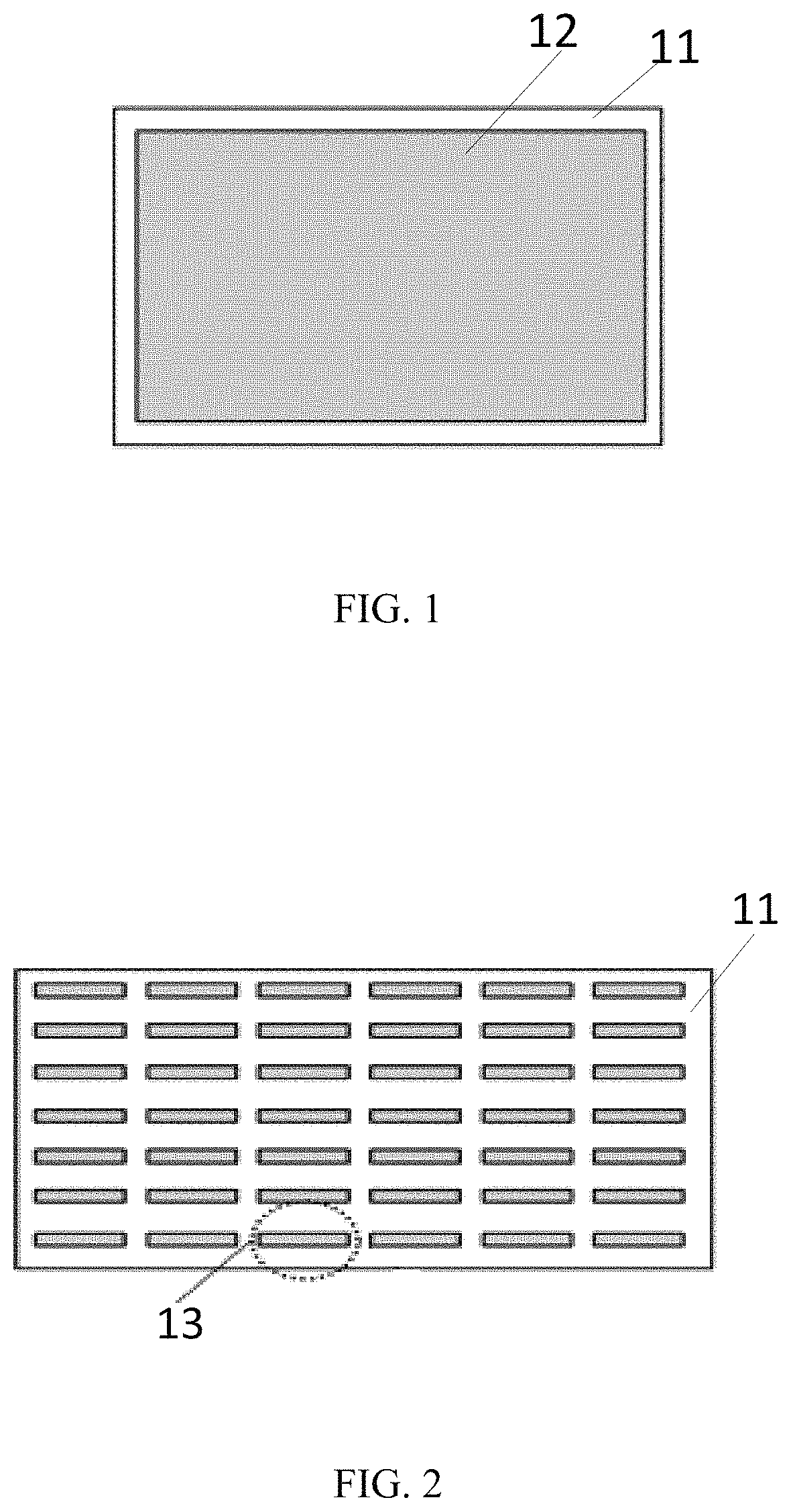
FIG. 1 is a schematic diagram of a first step of a manufacturing method of a flexible organic light emitting diode of the present disclosure.

As shown in FIG. 1, the manufacturing method of a flexible organic light emitting diode of the present disclosure includes:

S101, an amorphous silicon film is deposited over a flexible substrate.

As shown in FIG. 1, a barrier layer, a buffer layer, and the amorphous silicon film 12 a...


PUM

PropertyMeasurementUnit
flexibleaaaaaaaaaa
lengthaaaaaaaaaa
sizeaaaaaaaaaa

Abstract

A flexible organic light emitting diode display and manufacturing method thereof are provided. The method includes: performing a first patterning process on an amorphous silicon film; performing a crystallization treatment on the amorphous silicon film which has been processed by the first patterning process to form an oriented crystalline polycrystalline silicon film; performing a second patterning process on the polycrystalline silicon film to form a channel; and sequentially forming a gate, a source, a drain, an OLED display layer, and a packaging layer over the channel.

Description

FIELD OF THE DISCLOSUREThe present disclosure relates to the field of display devices, and more particularly to a flexible organic light emitting diode display and manufacturing method thereof.BACKGROUNDRecently, flexible display technology is mainly used in small and medium size products. In general, an LTPS-TFT back plane is used, where a low temperature poly-silicon (LTPS), which is crystallized by excimer laser annealing (ELA), serves as a channel layer of a thin film transistor (TFT). The electrical parameters (e.g., threshold voltage, subthreshold swing, mobility, etc.) of the TFT are strongly associated with a grain boundary density in the channel. To make an array substrate having good electrical uniformity, the LTPS film is required to have a very uniform grain size.An LTPS film is constituted by many silicon grains, which inevitably have grain boundaries. Since an atomic binding force at a crystalline interface of the LTPS thin film is weak, an inter-granular fracture / defo...

Claims


Application Information

Patent Timeline
Patent Type & Authority Patents(United States)
IPC IPC(8): H01L27/12H01L29/786H01L35/24H01L29/08H01L27/32H01L29/04H01L21/02H01L29/66H01L51/00
CPCH01L21/02595H01L27/1285H01L51/0097H01L29/04H01L27/1262H01L27/1218H01L29/78675H01L21/02532H01L29/66757H01L27/1222H01L27/1274H01L21/02675H01L21/02686H01L27/3244H01L2251/5338H01L2227/323H01L27/3262H10K59/1213H10K77/111H10K71/00Y02E10/549Y02P70/50H10K59/12H10K59/1201H10K2102/311
Inventor WANG, WEI
Owner WUHAN CHINA STAR OPTOELECTRONICS TECH CO LTD
Why Eureka
Try Eureka