Battery management chip circuit on the base of silicon on insulator (SOI) process

a technology of silicon on insulator and battery management, applied in secondary cell servicing/maintenance, battery technology, pulse technique, etc., can solve the problems of high-voltage leakage, inability to meet the requirements of high-voltage discharge, etc., to achieve the effect of improving reliability and stability, and reducing the power consumption of the chip

Active Publication Date: 2020-03-31
SHANGHAI INST OF MICROSYSTEM & INFORMATION TECH CHINESE ACAD OF SCI
View PDF7 Cites 0 Cited by
  • Summary
  • Abstract
  • Description
  • Claims
  • Application Information

AI Technical Summary

Benefits of technology

[0018]As described above, the battery management chip circuit on the basis of the SOI process provided by the present invention has the following beneficial effects:
[0019]1) The symmetric high-voltage MOS on the basis of the BCD process is a 6-end device, the corresponding SOI high-voltage device is a 4-end device, which decreases the difficulty and risk of chip design are decreased and reduces the wiring difficulty of layout design is reduced.
[0021]3) Trench isolation in the SOI process does not cause leakage current which is caused by PN junction isolation in the BCD process, and the power consumption of the chip is decreased.
[0022]4) In addition, the SOI process itself intrinsically has some advantages, including: high temperature is resisted, latching is resisted, and the reliability and stability of the chip are improved; the SOI device can effectively decrease the crosstalk between the devices, has certain radiation resistance and can be applied to fields of higher frequency such that the chip has a wider application field.

Problems solved by technology

In particular, both the LDWELL and BULK ports are not commonly used in common processes, voltage values need to be seriously considered in chip design.
In case of incomplete consideration or defects in simulation files, simulation software will not report errors, after the chip is taped out, problems of high-voltage leakage and even breakdown will be caused.
This is unacceptable for high cost of integrated circuit tape-out.

Method used


Image

  • Battery management chip circuit on the base of silicon on insulator (SOI) process
  • Battery management chip circuit on the base of silicon on insulator (SOI) process
  • Battery management chip circuit on the base of silicon on insulator (SOI) process

Examples


Embodiment Construction

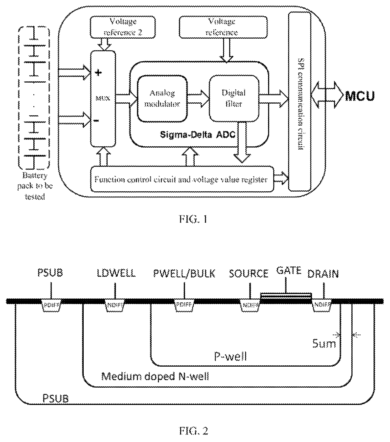
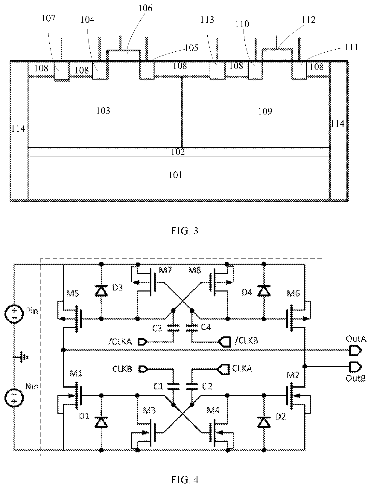
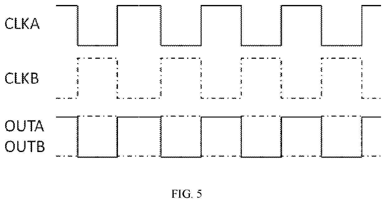
[0041]The embodiments of the present disclosure will be described below with reference to specific examples. Those skilled in the art can easily understand other advantages and effects of the present disclosure by the contents disclosed in the specification. The present disclosure can also be implemented or applied through other different specific embodiments. The details in the specification can also be on the basis of different viewpoints and applications, and various modifications or changes can be made without departing from the spirit of the present disclosure. Please refer to FIG. 1 and FIG. 3 to FIG. 5. It should be noted that the illustration provided in the embodiments merely illustrates the basic idea of the present disclosure in a schematic manner, only the components related to the present disclosure are shown in the illustration, the components are not drawn in accordance with actual number, shape and dimension, the form, quantity and proportion of the components can be...


PUM

PropertyMeasurementUnit
working voltageaaaaaaaaaa
voltageaaaaaaaaaa
voltageaaaaaaaaaa

Abstract

A battery management chip circuit on the basis of an SOI process. The battery management chip circuit comprises a high-voltage multiplexer MUX, a voltage reference circuit, a Sigma-delta ADC (comprising an analog modulator and a digital filter), an SPI communication circuit, a function control circuit and a voltage value register. The battery management chip circuit is integrated on the basis of an SOI high-voltage process, and particularly, high-voltage MOS transistors adopted by the battery management chip circuit are high-voltage MOS device units on the basis of the SOI process. In addition, the present invention highlights the design of interface circuit-chopper circuit of the high-voltage multiplexer MUX and the Sigma-delta ADC, so as to describe the advantages such as decrease of difficulty of circuit design and reduction of layout area brought about when the present invention adopts the SOI process design and tape-out.

Description

CROSS REFERENCE TO RELATED PATENT APPLICATION[0001]The present application is the US national stage of PCT / CN2016 / 088056 filed on Jul. 1, 2016, which claims the priority of the Chinese patent application No. CN201610150614.7 filed on Mar. 16, 2016, which application is incorporated herein by reference.BACKGROUND OF THE PRESENT INVENTIONField of Invention[0002]The present invention relates to a battery management chip circuit, in particular to a battery management chip circuit on the basis of a silicon on insulator (SOI) process.Description of Related Arts[0003]Electric vehicles will use lithium batteries as main power drive sources in future. A BMS (Battery Management System) is a key part which is used for guaranteeing normal working of lithium batteries and mainly comprises a battery voltage conversion and measurement circuit, a battery balance drive circuit, a switch drive circuit, a current measurement and communication circuit, and corresponding rear-end data processing modules...

Claims


Application Information

Patent Timeline
Patent Type & Authority Patents(United States)
IPC IPC(8): H01L25/00H03K17/693H03K17/567H01L29/06H01L21/762H01L21/761H01L29/78H01M10/42H01L27/12H03K17/687H01L27/092
CPCH01L29/78H01M10/4257H01M10/42H01L27/1203H01M10/4264H03K17/693H01L21/761H01L21/76283H03K17/567H03K17/6872H01L29/0653H01M2220/20H01L27/092H01M2010/4271H01L27/02H01M10/425Y02E60/10
Inventor CHENG, XINHONGLI, XINCHANGWU, ZHONGHAOXU, DAWEIYU, YUEHUI
Owner SHANGHAI INST OF MICROSYSTEM & INFORMATION TECH CHINESE ACAD OF SCI
Why Eureka
Try Eureka