
Light receiving device, method of manufacturing light receiving device, imaging device, and electronic apparatus

a technology of light receiving device and light receiving device, which is applied in the direction of color television, television system, radio control device, etc., can solve the problems of reduced dynamic range of obtained image, dark current, etc., and achieves large noise, large potential gradient, and high defect density

Active Publication Date: 2020-04-14
SONY CORP
View PDF16 Cites 0 Cited by
  • Summary
  • Abstract
  • Description
  • Claims
  • Application Information

AI Technical Summary

Benefits of technology

This patent describes a method to improve the quality of images captured using a light receiving device. The method involves the use of a covering layer made of a specific material called a Group IV semiconductor that is placed on top of the photoelectric conversion layer. This covering layer helps to reduce defects and dark current, which can affect image quality. By using this technique, the light receiving device can capture images with greater clarity and accuracy.

Problems solved by technology

Here, an interface between a compound semiconductor and the insulating film is high in defect density, and therefore such an interface defect causes a dark current.
Further, a larger noise leads to a smaller S / N ratio, resulting in reduction in a dynamic range of an obtained image as well.

Method used


Image

  • Light receiving device, method of manufacturing light receiving device, imaging device, and electronic apparatus
  • Light receiving device, method of manufacturing light receiving device, imaging device, and electronic apparatus
  • Light receiving device, method of manufacturing light receiving device, imaging device, and electronic apparatus

Examples


modification example 1

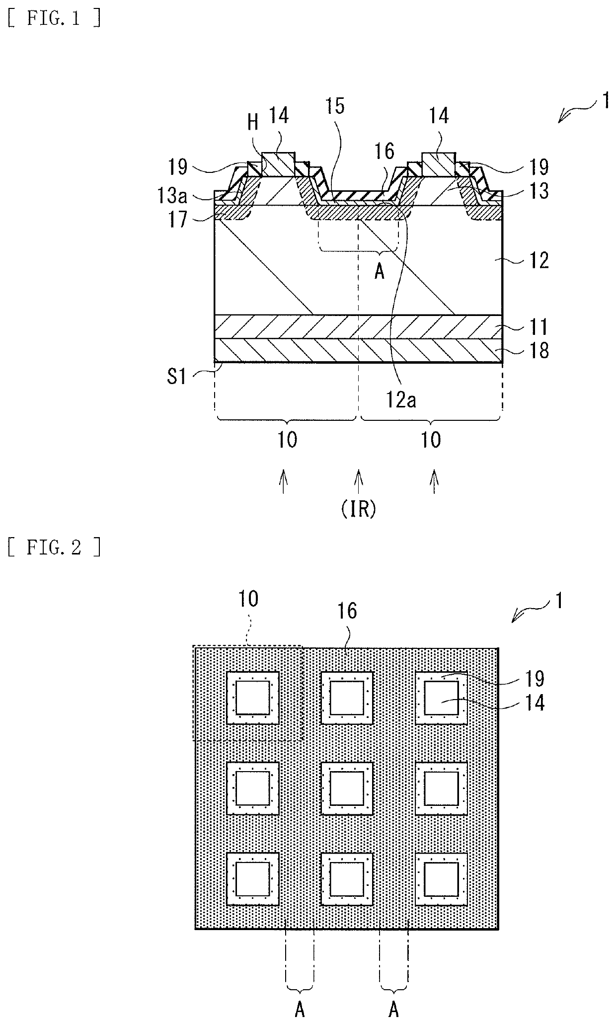
[0087]FIG. 9 illustrates a cross-sectional configuration of a light receiving device (a light receiving device 1A) according to a modification example 1. As with the above-described embodiment, the light receiving device 1A includes, for example, the photoelectric conversion layer 12 and the plurality of contact layers 13 in this order on the substrate 11, and the plurality of contact layers 13 are provided on the photoelectric conversion layer 12 at the spacing intervals A with respect to one another. The first electrode 14 is electrically coupled to each of the plurality of contact layers 13 through the opening H of the mask layer 19. A covering layer (a covering layer 15A) and insulating films (insulating films 16A and 16) are formed in this order to cover a portion (the surface 12a) of the front surface of the photoelectric conversion layer 12 and the side surface 13a of each of the contact layers 13. A diffusion region (a diffusion region 17A) including an impurity is formed in...

modification example 2

[0091]FIG. 10 illustrates a cross-sectional configuration of a light receiving device (a light receiving device 1B) according to a modification example 2. As with the above-described embodiment, the light receiving device 1B includes, for example, the photoelectric conversion layer 12 and the plurality of contact layers 13 in this order on the substrate 11, and the plurality of contact layers 13 are provided on the photoelectric conversion layer 12 at the spacing intervals A with respect to one another. The first electrode 14 is electrically coupled to each of the plurality of contact layers 13 through the opening H of the mask layer 19. A covering layer (a covering layer 15B) and the insulating film 16 are formed in this order to cover a portion (the surface 12a) of the front surface of the photoelectric conversion layer 12 and the side surface 13a of each of the contact layers 13. A diffusion region (a diffusion region 17B) including an impurity is formed in a region adjacent to t...

modification example 3

[0095]FIG. 11 illustrates a cross-sectional configuration of a light receiving device (a light receiving device 1C) according to a modification example 3. As with the above-described embodiment, the light receiving device 1C includes, for example, the photoelectric conversion layer 12 and the plurality of contact layers 13 in this order on the substrate 11, and the plurality of contact layers 13 are provided on the photoelectric conversion layer 12 at the spacing intervals A with respect to one another. The first electrode 14 is electrically coupled to each of the plurality of contact layers 13 through the opening H of the mask layer 19. A covering layer (a covering layer 15C) and the insulating film 16 are formed in this order to cover a portion (the surface 12a) of the front surface of the photoelectric conversion layer 12 and the side surface 13a of each of the contact layers 13. The diffusion region 17 is formed in a region adjacent to the covering layer 15C of the photoelectric...


PUM

PropertyMeasurementUnit
thicknessaaaaaaaaaa
wavelengthaaaaaaaaaa
electrical chargeaaaaaaaaaa

Abstract

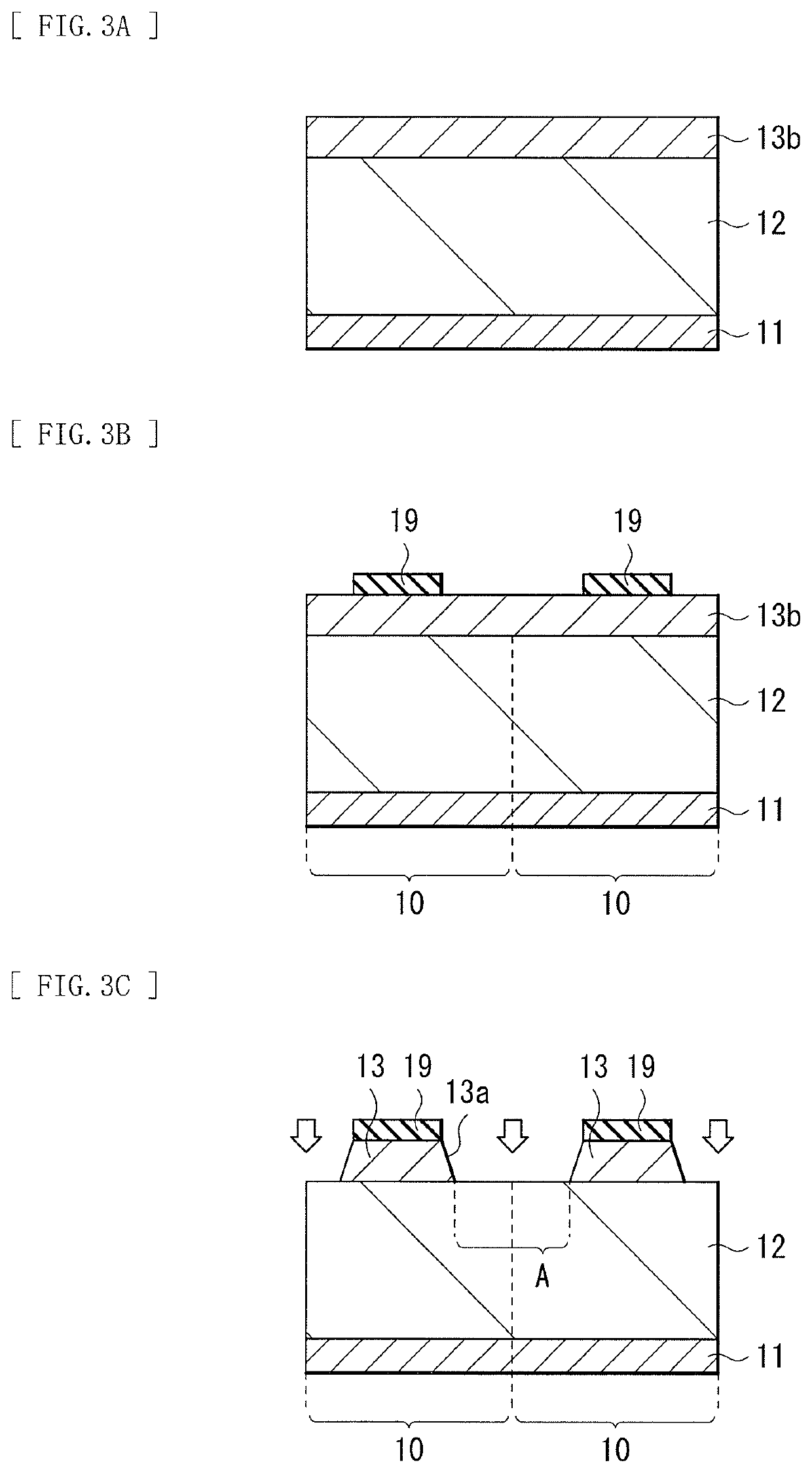
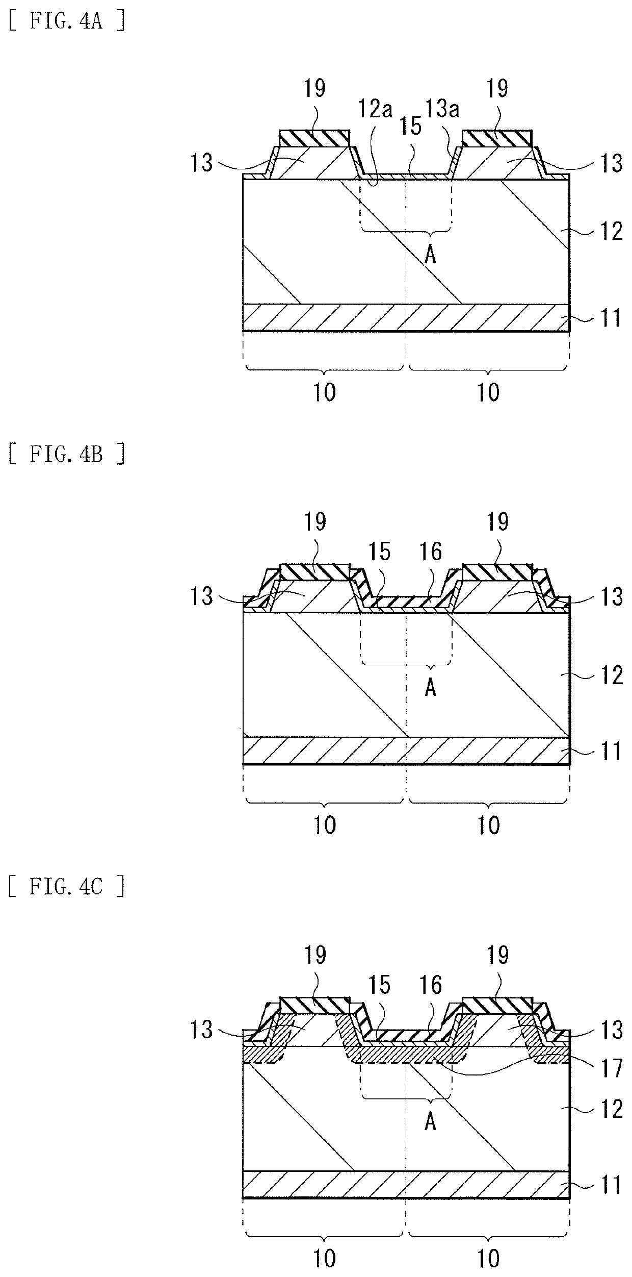
A light receiving device includes: a photoelectric conversion layer that includes a first compound semiconductor, and absorbs a wavelength in an infrared region to generate electrical charges; a plurality of contact layers that include a second compound semiconductor, and are provided on the photoelectric conversion layer at spacing intervals with respect to one another; and a covering layer that is formed to cover a portion corresponding to the spacing intervals of a front surface of the photoelectric conversion layer and side surfaces of the respective contact layers, and includes a Group IV semiconductor.

Description

CROSS REFERENCE TO RELATED APPLICATIONS[0001]This application is a national stage application under 35 U.S.C. 371 and claims the benefit of PCT Application No. PCT / JP2016 / 083857 having an international filing date of 15 Nov. 2016, which designated the United States, which PCT application claimed the benefit of Japanese Patent Application No. 2016-008460 filed 20 Jan. 2016, the entire disclosures of each of which are incorporated herein by reference.TECHNICAL FIELD[0002]The present disclosure relates to a light receiving device that is able to detect, for example, infrared light and a method of manufacturing the same, and to an imaging device and an electronic apparatus.BACKGROUND ART[0003]In recent years, research and development of an infrared sensor has been carried out for the purpose of monitoring, military applications, etc. As a light receiving device used for such an infrared sensor, a light receiving device is proposed that uses, for example, any of compound semiconductors (...

Claims


Application Information

Patent Timeline
Patent Type & Authority Patents(United States)
IPC IPC(8): H01L27/146H04N5/33H01L31/10H01L31/0264H01L31/02H01L27/144H01L31/0328H01L31/18H04N5/369
CPCH01L31/0328H01L31/10H01L27/14649H01L31/0264H01L27/14623H01L27/144H04N5/33H04N5/369H01L27/146H01L31/1864H01L31/02Y02E10/50H04N25/70H04N23/20
Inventor MINARI, HIDEKIMARUYAMA, SHUNSUKE
Owner SONY CORP
Learn More