Preparation method of SOI (Silicon-On-Insulator) substrate material and SOI material

A technology of substrate materials and silicon substrates, applied in semiconductor/solid-state device manufacturing, electrical components, electrical solid-state devices, etc., can solve the problems of low substrate surface resistivity, affecting device performance, and easy introduction of impurities, etc. Effects of RF substrate loss, increased linearity, and simple process

Inactive Publication Date: 2018-03-09
SHENYANG SILICON TECH
View PDF4 Cites 5 Cited by
  • Summary
  • Abstract
  • Description
  • Claims
  • Application Information

AI Technical Summary

Problems solved by technology

[0005] 3. High-resistance SOI substrate: This type of substrate has structural advantages, but its performance is worse than that of the first type
However, diffusion of oxygen atoms, heat treatment process lead to low surface resistivity of the formed substrate
These two reasons are currently out of control
[0007] 4. On the basis of the third type, the high-resistance SOI substrate type substrate is improved by adding a defect layer. The conventional defect layer growth is easy to introduce impurities, which affects the final performance of the device.

Method used


Image

  • Preparation method of SOI (Silicon-On-Insulator) substrate material and SOI material
  • Preparation method of SOI (Silicon-On-Insulator) substrate material and SOI material
  • Preparation method of SOI (Silicon-On-Insulator) substrate material and SOI material

Examples


Embodiment 1

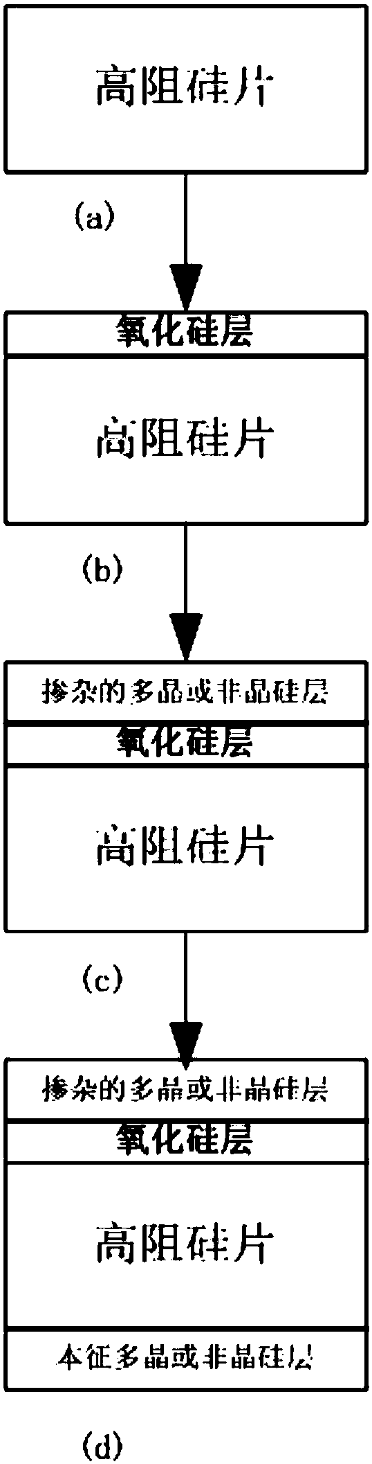
[0044] This embodiment provides a kind of preparation method of SOI silicon substrate material and SOI material, and this substrate refers to the SOI substrate sheet with intrinsic polycrystalline or intrinsic amorphous silicon layer on the back, and its preparation comprises the following steps:

[0045] 1. Provide high-resistance silicon wafers (silicon wafer resistivity greater than 500ohm.cm), and use DHF, SC1 and SC2 to clean the surface in order to remove the natural oxide layer and pollutants on the silicon wafer surface ( figure 1 (a)).

[0046] 2. Reference figure 1 (b), prepare a silicon oxide layer on the surface of the high-resistance silicon wafer, the thickness of the grown oxide layer

[0047] 3. In figure 1 On the basis of (b), prepare a doped polysilicon layer ( figure 1 (c)), the thickness is 2 μm, the doping type is P type, and the resistivity is 1ohm.cm.

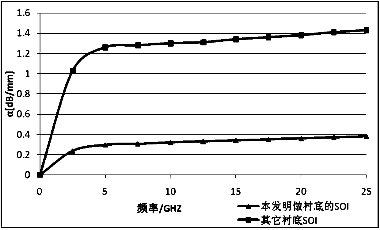
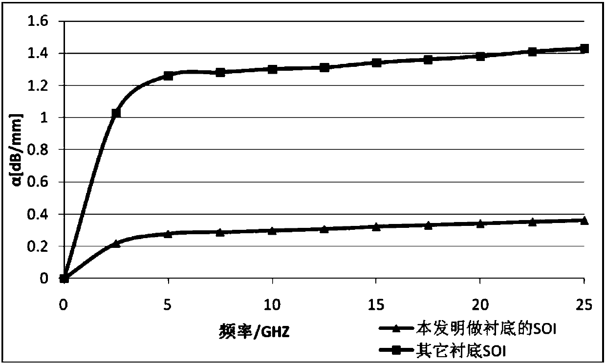
[0048] 4. In figure 1 On the basis of (c), a 2 μm intrinsic polysilicon layer is grown on the b...

Embodiment 2

[0052] This embodiment provides a method for preparing an SOI silicon substrate, which refers to an SOI substrate with an intrinsic polycrystalline or intrinsic amorphous silicon layer on the back, and its preparation includes the following steps:

[0053] 1. Provide high-resistance silicon wafers (silicon wafer resistivity greater than 500ohm.cm), and use DHF, SC1 and SC2 to clean the surface in order to remove the natural oxide layer and pollutants on the silicon wafer surface ( figure 1 (a)).

[0054] 2. Reference figure 1 (b), prepare a silicon oxide layer on the surface of the high-resistance silicon wafer, the thickness of the grown oxide layer

[0055] 3. In figure 1 On the basis of (b), prepare a doped polysilicon layer ( figure 1 (c)), the thickness is 2 μm, the doping type is P type, and the resistivity is 1ohm.cm.

[0056] 4. In figure 1 On the basis of (c), a 2 μm intrinsic amorphous silicon layer is grown on the back. ( figure 1 (d))

[0057] 5. Use fig...


PUM

PropertyMeasurementUnit
thicknessaaaaaaaaaa
thicknessaaaaaaaaaa

Abstract

The invention discloses a preparation method of an SOI substrate material and an SOI material and belongs to the SOI wafer preparation technical field. An intrinsic polycrystalline or amorphous silicon layer is grown on the back surface of an SOI substrate wafer provided with a doped polycrystalline layer or doped amorphous silicon layer, so that the substrate material can be formed; the SOI material is made of the SOI substrate material; the doped polycrystalline layer or doped amorphous silicon layer is combined with silicon oxide, so that higher defect density can be realized, and therefore, capacitance variation can be limited, and the power of generated harmonics can be reduced; and since the intrinsic polycrystalline or amorphous silicon layer is grown on the back surface, so that impurities introduced during a doping process can be decreased, and therefore, the RF substrate loss of the high-resistance SOI substrate can be reduced, the linear characteristics of the substrate canbe increased, direct-current voltage bias can be decreased, the high-resistance SOI substrate can be compatible with a CMOS, and the loss of radio frequency can be decreased.

Description

technical field [0001] The invention relates to the technical field of preparation of SOI sheets, in particular to a method for preparing an SOI silicon substrate material and an SOI material. The prepared silicon substrate is mainly used in radio frequency equipment. Background technique [0002] The materials currently used for RF front-end modules are as follows: [0003] 1. SOQ (silicon on silicon on quartz), SOS (silicon on sapphire sapphire): SOQ is the same as traditional SOI, it produces lower leakage current, due to its lower parasitic capacitance, high frequency Circuit performance has been improved. The advantage of SOS is its excellent electrical insulation, which can effectively prevent the radiation caused by stray currents from spreading to nearby components. Substrates such as SOQ and SOS can achieve excellent RF performance, but there are very few such structures, so they are very expensive. [0004] 2. High-resistance substrate silicon: its resistivity i...

Claims


Application Information

Patent Timeline
Patent Type & Authority Applications(China)
IPC IPC(8): H01L21/762H01L27/12
Inventor 李捷高文琳
Owner SHENYANG SILICON TECH
Why Eureka
Try Eureka